Wafer level chip packaging method

A wafer-level chip and packaging method technology, which is applied in the manufacturing of electrical components, electrical solid-state devices, semiconductor/solid-state devices, etc., can solve problems such as easy falling off of low-temperature oxide layers

CN104733328AActive Publication Date: 2015-06-24SEMICON MFG INT (SHANGHAI) CORP +1
4 Cites 0 Cited by

Patent Information

Authority / Receiving Office
CN · China
Current Assignee / Owner
Publication Date
2015-06-24

Smart Images

  • Figure 1
    Figure 1
  • Figure 2
    Figure 2
  • Figure 3
    Figure 3
Patent Text Reader

Abstract

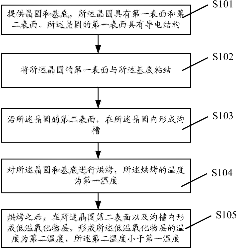
A wafer level chip packaging method comprises the following steps: providing a wafer and a substrate, wherein the wafer has a first surface and a second surface, and the first surface of the wafer is provided with a conductive structure; bonding the first surface of the wafer with the substrate; forming a trench in the wafer along the second surface of the wafer; baking the wafer and the substrate, wherein the baking temperature is a first temperature; and after baking, forming a low-temperature oxide layer on the second surface of the wafer and in the trench, wherein the temperature at which the low-temperature oxide layer is formed is a second temperature which is lower than the first temperature. By adopting the packaging method, the problem that the low-temperature oxide layer falls off the surface of the wafer can be avoided.
Need to check novelty before this filing date? Find Prior Art

Description

technical field

[0001] The invention relates to the technical field of semiconductors, in particular to a wafer-level packaging method. Background technique

[0002] Wafer Level Packaging (WLP) is a kind of chip packaging method. After the whole wafer is produced, it is packaged and tested directly on the wafer. After the completion, it is cut into a single chip. After punching or filling. Wafer-level packaging has the advantages of small package size and excellent electrical performance after packaging. Wafer-level packaging is also easily compatible with wafer manufacturing and chip assembly, simplifying the process from wafer manufacturing to product shipment, and reducing overall production costs.

[0003] However, it has been found in practice that the low-temperature oxide layer used in the wafer-level packaging structure is easy to fall off.

[0004] Therefore, improvements in wafer-level packaging methods are needed. Contents of the invention

[0005] The proble...

Examples

Embodiment Construction

[0033] In the existing wafer-level packaging method, it is necessary to form a layer of low-temperature oxide layer on the surface of the semiconductor wafer as an isolation layer, so as to isolate the wafer from the conductive structure subsequently formed on the surface of the semiconductor wafer. However, it is found in the actual manufacturing process that the bonding strength between the isolation layer formed on the surface of the semiconductor wafer and the semiconductor wafer by using the existing technology is poor, and the phenomenon that the isolation layer peels off from the semiconductor wafer often occurs, which seriously reduces the Stability of semiconductor devices formed after packaging.

[0034] After research, it is found that in the existing wafer-level chip packaging method, the reason why the low-temperature oxide layer on the surface of the wafer is easy to peel off is:

[0035] In the existing wafer-level chip packaging method, the adhesive used to bon...