

Piezoelectric device and manufacturing method thereof, electronic device and control method
A technology for piezoelectric devices and electronic devices, which is applied in the field of piezoelectric devices and can solve the problems of being unable to form bendable piezoelectric devices and not being bendable
Patent Information
- Authority / Receiving Office
- CN · China
- Current Assignee / Owner
- Publication Date
- 2020-07-24
Smart Images
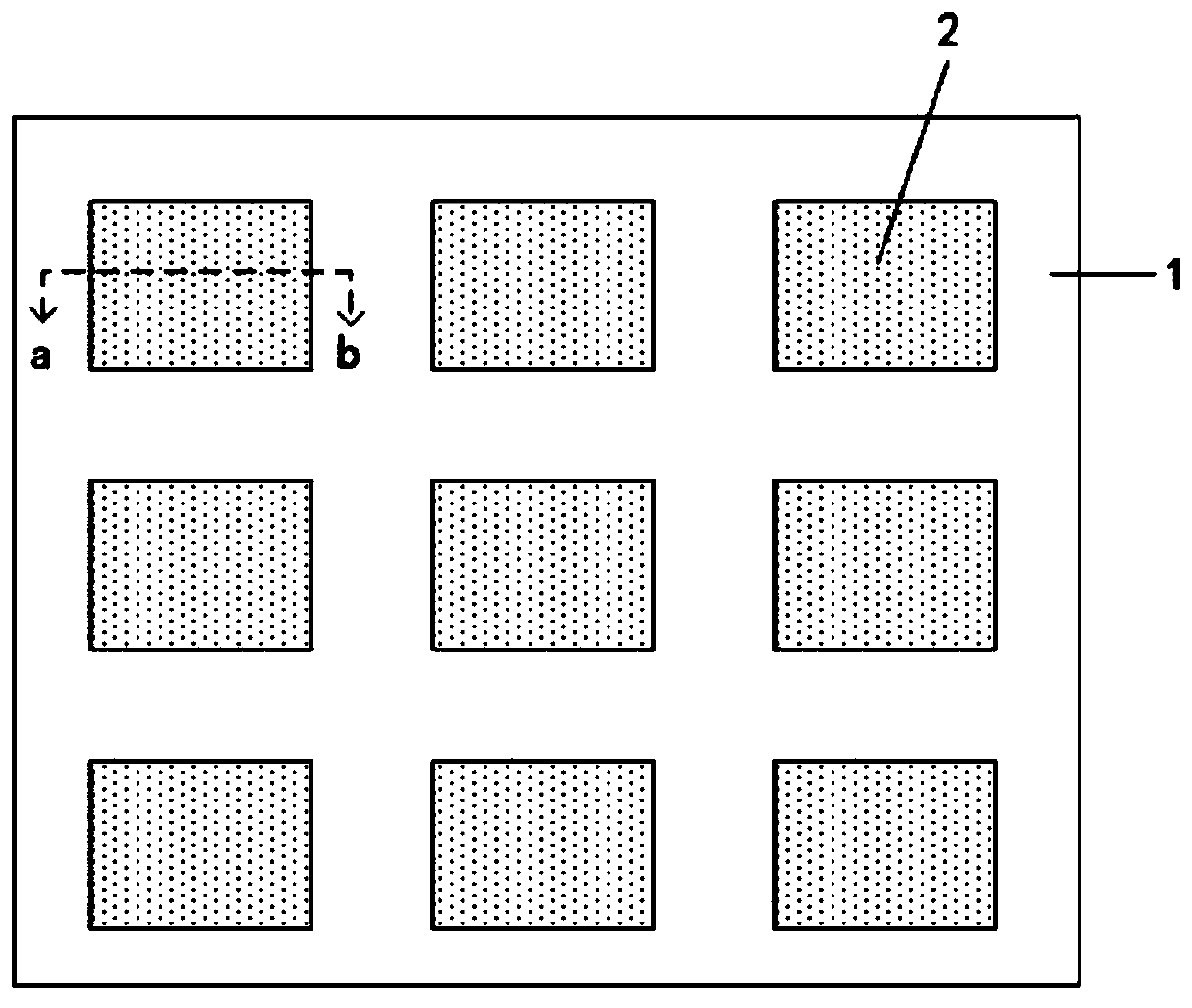
Figure 1 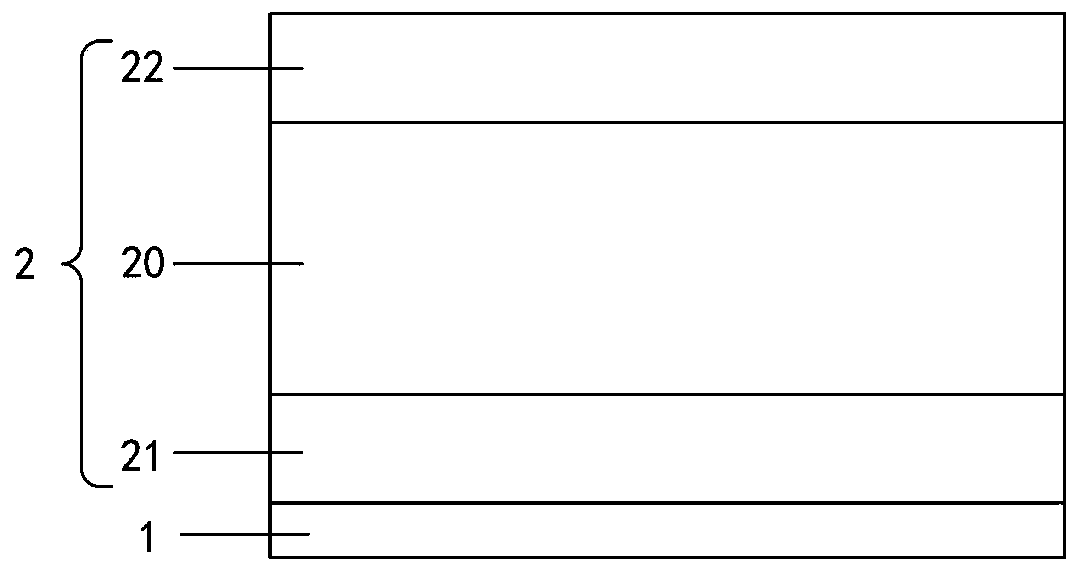
Figure 2 
Figure 3
Abstract
Description
technical field
[0001] The invention relates to the technical field of piezoelectric devices, in particular to a piezoelectric device, a manufacturing method thereof, an electronic device and a control method. Background technique
[0002] Piezoelectric devices refer to devices made using the piezoelectric effect of materials and have a very wide range of applications. At present, piezoelectric materials in piezoelectric devices are mostly made of piezoelectric ceramics. Piezoelectric ceramics have very good piezoelectric performance, but they are not bendable and cannot form bendable piezoelectric devices. Contents of the invention
[0003] Embodiments of the present invention provide a piezoelectric device and its manufacturing method, an electronic device and a control method. The piezoelectric device has bendability and can be bent.
[0004] In order to achieve the above object, embodiments of the present invention adopt the following technical solutions:
[0005] I...
Examples
Embodiment 1
[0059] An embodiment of the present invention provides a piezoelectric device, referring to figure 1 As shown, the piezoelectric device includes: a flexible substrate 1 and a plurality of piezoelectric units 2 disposed on the flexible substrate 1 and arranged in an array. refer to figure 2 As shown, each piezoelectric unit 2 includes: a first electrode 21 , a piezoelectric part 20 and a second electrode 22 sequentially stacked on the flexible substrate 1 ; the material of the piezoelectric part is a rigid material.
[0060] The material of the flexible substrate is not limited here. For example, the material of the flexible substrate can be PI (Polyimide, polyimide), PET (Polyethylene Terephthalate, polyethylene terephthalate) or PDMS (Polydimethylsiloxane ,Polydimethylsiloxane).
[0061] The above-mentioned first electrode may only include one electrode layer, and the material of the electrode layer may be a single metal or multiple metals. Exemplarily, the material of th...
Embodiment 2
[0085] An embodiment of the present invention provides an electronic device, including: a plurality of switch units and the above-mentioned piezoelectric device; the plurality of switch units are electrically connected to the plurality of piezoelectric units of the piezoelectric device in one-to-one correspondence, and are configured to control the piezoelectric unit voltage.
[0086] The specific structure of the switch unit is not limited here. Figure 7 In FIG. 1 , a switching unit including a thin film transistor (ThinFilm Transistor, TFT) is taken as an example for illustration. Figure 7 Among them, a plurality of thin film transistors 3 are electrically connected to a plurality of piezoelectric units 2 of the piezoelectric device in a one-to-one correspondence. refer to Figure 8 As shown, the piezoelectric unit 2 in the piezoelectric device can be bound to the PI film 4 (that is, the PI-TFT backplane) provided with a plurality of TFT3 through the binding layer 5 (Bon...
Embodiment 3
[0101] An embodiment of the present invention provides a method for manufacturing a piezoelectric device as described in Embodiment 1, the method comprising:
[0102] S01. Fabricate a first substrate; the first substrate includes a flexible substrate and a plurality of first electrodes disposed on the flexible substrate.
[0103] S02 , making a second substrate; the second substrate includes a rigid substrate, and a plurality of piezoelectric parts and a plurality of second electrodes sequentially stacked on the rigid substrate; the material of the piezoelectric part is a rigid material.
[0104] S03 , peeling off the plurality of piezoelectric parts and the plurality of second electrodes of the second substrate.
[0105] For example, laser peeling and other methods can be used for peeling.
[0106] S04 , binding the stripped multiple piezoelectric parts and multiple second electrodes to the first substrate to obtain multiple piezoelectric units arranged in an array.
[0107...