
Optical device, method of manufacturing the same, and electronic apparatus
a manufacturing method and optical device technology, applied in the direction of semiconductor/solid-state device manufacturing, electrical equipment, semiconductor/solid-state devices, etc., can solve the problems of warpage, deterioration of resistance to moisture and impact, and weakening of bonding strength, so as to maintain yield and design flexibility of optical devices, reduce warpage, and maintain bonding strength
- Summary
- Abstract
- Description
- Claims
- Application Information
AI Technical Summary
Benefits of technology
Problems solved by technology
Method used
Image

Examples
embodiment 1
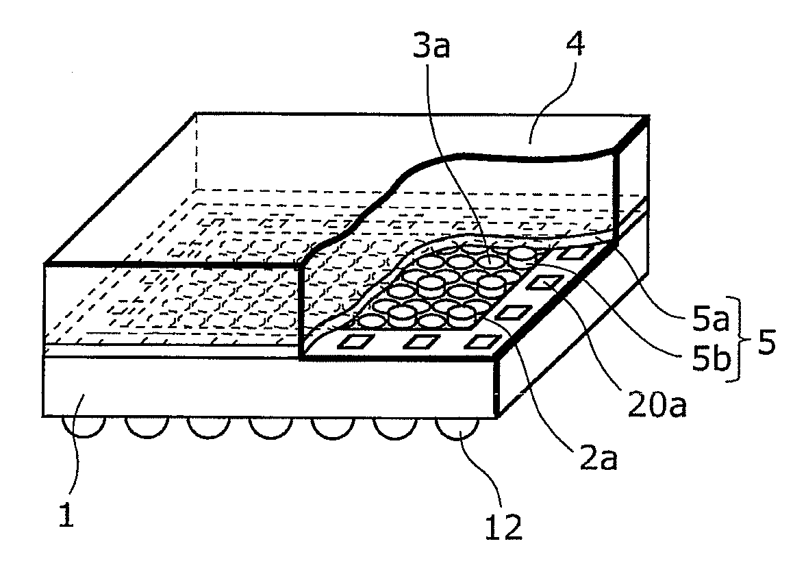
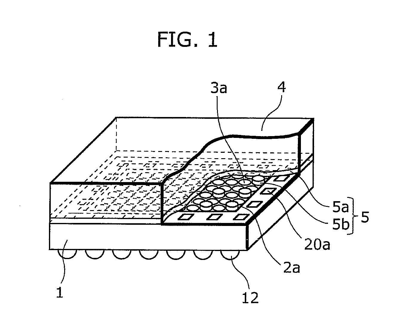
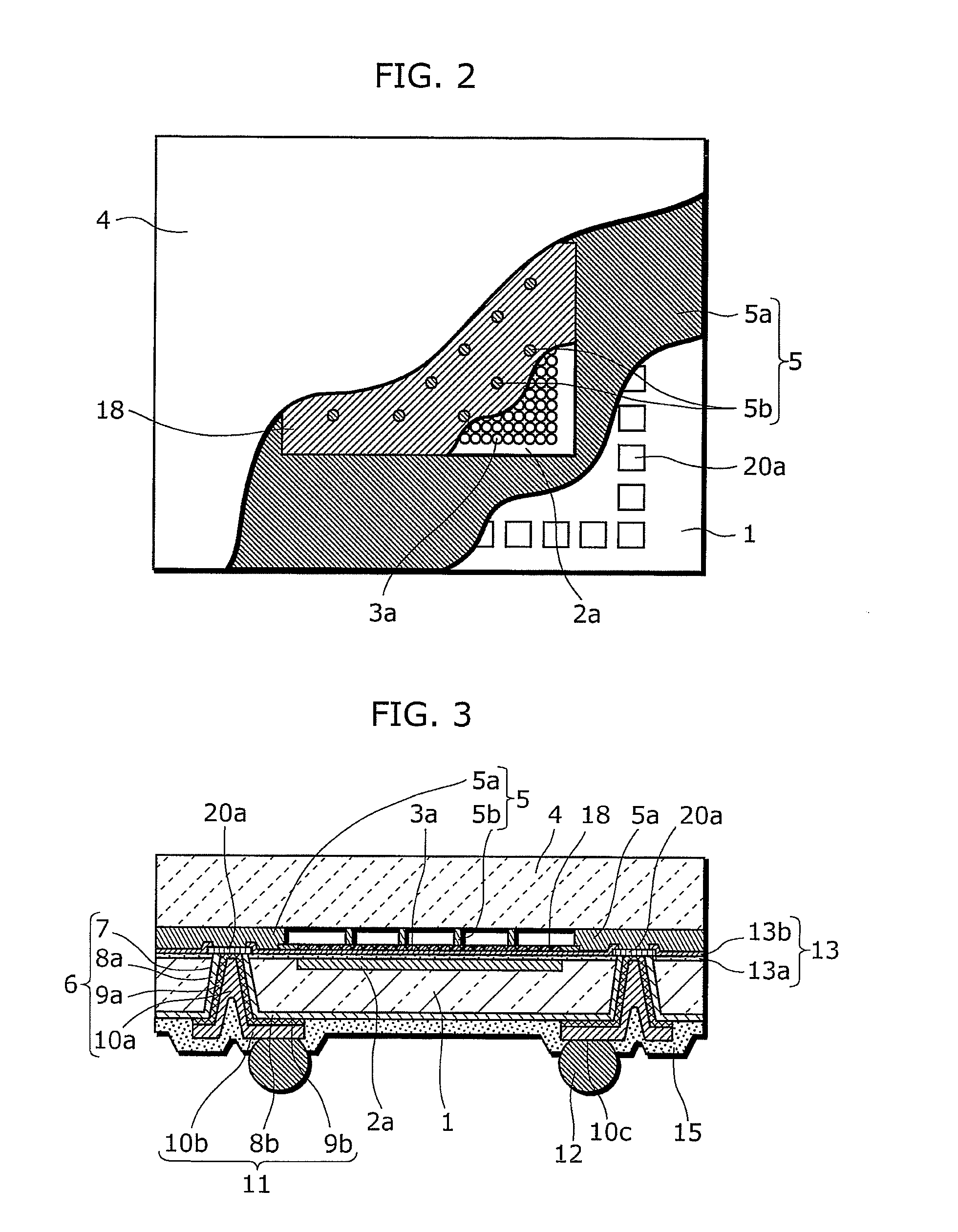
[0065]FIG. 1 to FIG. 3 show a structure of a CMOS solid-state imaging device which is a typical optical device according to Embodiment 1 of the present invention, and are respectively a perspective view, a plan view, and a sectional view illustrating the CMOS solid-state imaging device.
[0066]As shown in FIG. 1 to FIG. 3, the solid-state imaging device according to Embodiment 1 is a solid-state imaging device having through electrodes. In the solid-state imaging device, in semiconductor processing, a light-receiving unit (pixel unit) 2a including one or more unit pixels (not shown) is formed in one surface (top surface) of a semiconductor substrate 1, and peripheral circuitry (not shown) is formed in a peripheral part of the semiconductor substrate 1 through semiconductor processes. Each of the unit pixels includes light-receiving elements (not shown), which is an optical element, and one or more active elements (not shown). The peripheral circuitry includes a circuit mainly for cont...
embodiment 2
[0156]FIG. 22 is a sectional view illustrating a structure of a CMOS solid-state imaging device as an example of an optical device which has structure in which lateral electrodes are included according to Embodiment 2 of the present invention.
[0157]As shown in FIG. 22, the solid-state imaging device according to Embodiment 2 is a solid-state imaging device with lateral electrodes. In the solid-state imaging device, lateral electrodes 6a formed on a lateral surface of the semiconductor substrate 1 each electrically connect an electrode 20a and an external terminal 12. The electrode 20a is electrically connected with elements above one surface in which a light-receiving unit 2a of the semiconductor substrate 1 is formed. The external terminal 12 is provided on the other surface of the semiconductor substrate 1. Each of the lateral electrodes 6a include an insulating film 8a provided in contact with the lateral surface of the semiconductor substrate 1, a conducting film 9a provided in ...
embodiment 3
[0161]FIG. 23A is a sectional view illustrating a structure of a CMOS solid-state imaging device as an example of an optical device according to Embodiment 3 of the present invention.
[0162]As shown in FIG. 23A, the solid-state imaging device according to Embodiment 3 is a back-side illumination solid-state imaging device. In the solid-state imaging device, a semiconductor substrate 1 is formed to have a thin thickness, and elements and wiring 20 electrically connected to the elements are formed not on one surface (top surface) in which the light-receiving unit 2a is formed but on a side of the other surface (bottom surface) of the semiconductor substrate 1. An electrode 20a formed on one end of the wiring 20 is electrically connected to an external terminal 12 on the side of the bottom surface of the semiconductor substrate 1 by a through plug 29. On the top surface side of the semiconductor substrate 1, an insulating film 13c is formed. The light-receiving elements in the light-rec...
PUM
 Abstract
Description
Claims
Application Information