
Polarization insensitive array wave-guide grating
An arrayed waveguide grating, polarization-insensitive technology, applied in the coupling of optical waveguides, etc., can solve the problems of unsuitable silicon nanowire arrayed waveguide gratings, etc., and achieve the effect of convenient design and simple structure
Patent Information
- Authority / Receiving Office
- CN · China
- Current Assignee / Owner
- Publication Date
- 2008-07-09
- Estimated Expiration
- Not applicable · inactive patent
Smart Images
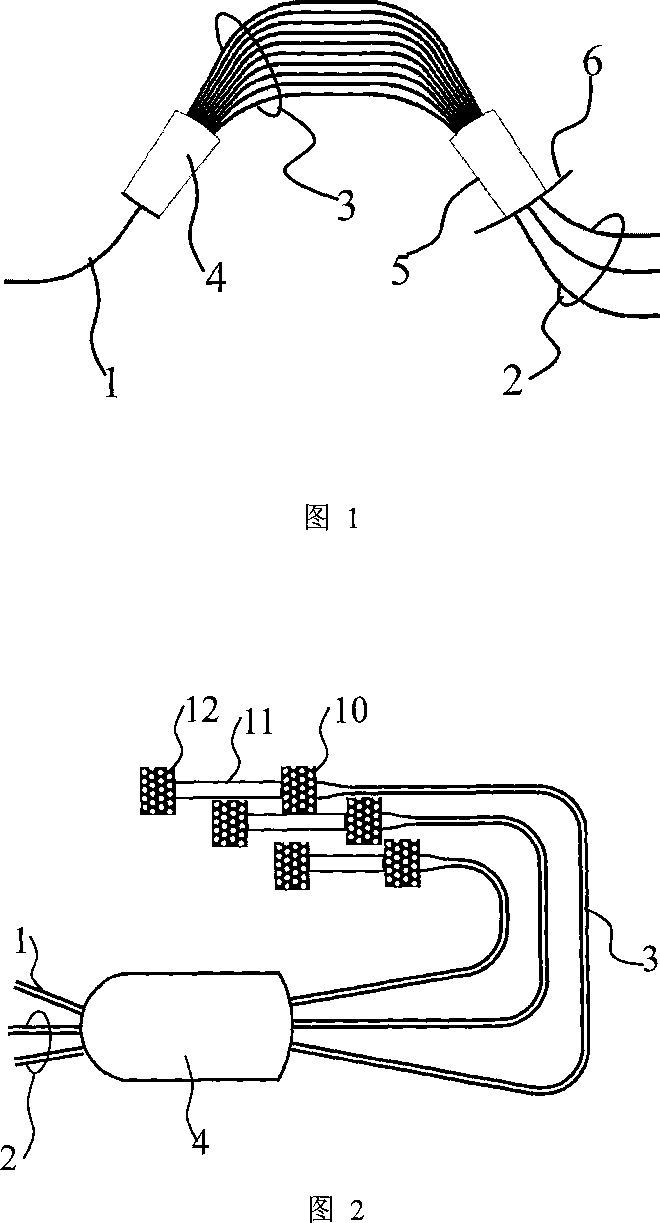
Figure 1
Abstract
Description
technical field
[0001] The invention relates to a polarization-insensitive arrayed waveguide grating, which belongs to the field of planar optical waveguide integrated devices. Background technique
[0002] Wavelength division multiplexing / demultiplexing is a key modern optical communication technology. Its function is to mix light of different wavelengths into composite light or to separate the light of each wavelength contained in the composite light. The device that realizes this function is the wavelength division multiplexing / demultiplexing device. Arrayed waveguide grating is a typical integrated wavelength division multiplexing / demultiplexing device. The traditional arrayed waveguide grating is composed of input waveguide 1, input slab waveguide 4, arrayed waveguide 3, output slab waveguide 5 and output waveguide 2. (See Figure 1), the composite light is incident from the input waveguide, enters the slab waveguide and propagates divergently, and then couples to each ...
Examples
Embodiment Construction
[0013] Referring to Fig. 2, the polarization-insensitive arrayed waveguide grating of the present invention comprises an input waveguide 1, an output waveguide 2, a slab waveguide 4 and several arrayed waveguides 3, the input waveguide 1 and the output waveguide 2 are located on the same side of the slab waveguide 4, and The slab waveguides 4 are connected, and the other side of the slab waveguides 4 is connected to one end of each arrayed waveguide 3, and there is an optical path difference ΔL between adjacent arrayed waveguides 1 , the other end of each arrayed waveguide is sequentially connected to the polarizing beam splitter 10 and the mirror 12, there is a connecting waveguide 11 between the polarizing beam splitter 10 and the reflecting mirror 12, and there is an optical path difference ΔL between adjacent connecting waveguides 11 2 .
[0014] A specific embodiment is given below.
[0015] In this example, the refractive indices of the core layer, lower cladding layer,...