
Thin film transistor in liquid crystal display and manufacturing method thereof
A technology of liquid crystal display devices and thin film transistors, applied in the direction of transistors, semiconductor/solid-state device manufacturing, electric solid-state devices, etc., can solve the problems of leakage current and large coupling capacitance, and achieve the elimination of leakage current, increase in width, and good uniformity Effect
Patent Information
- Authority / Receiving Office
- CN · China
- Patent Type
- Applications(China)
- Current Assignee / Owner
- Publication Date
- 2009-12-02
- Estimated Expiration
- Not applicable · inactive patent
Smart Images
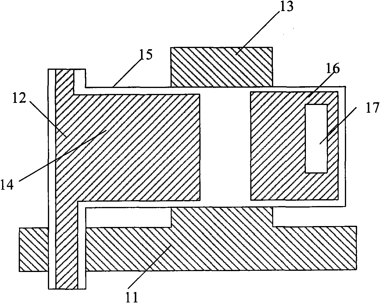
Figure 1 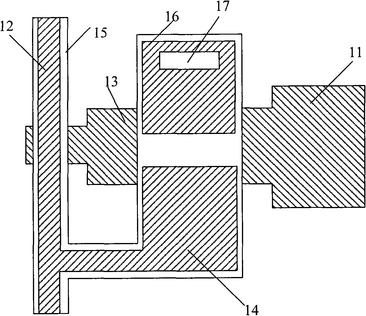
Figure 2 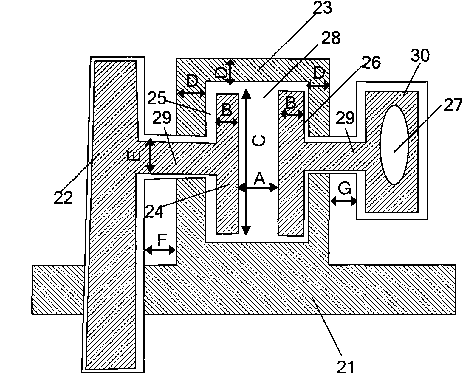
Figure 3
Abstract
Description
technical field
[0001] The invention relates to a liquid crystal display device, in particular to a thin film transistor in the liquid crystal display device and a manufacturing method thereof. Background technique
[0002] Thin film transistor liquid crystal display devices have gradually occupied the vast majority of the display market due to their advantages of thinness, lightness, power saving, and environmental protection. In the liquid crystal display device, it is the liquid crystal panel that plays a decisive role in the quality. On the array substrate of the liquid crystal display panel, a very important component is the thin film transistor connecting the gate scanning line, the data line and the pixel electrode. The most widely used thin film transistor structures are figure 1 shown in portrait orientation and figure 2 Two orientations are shown. from figure 1 , figure 2 It can be seen from the figure that the thin film transistor in the liquid crystal disp...
Examples
Embodiment 1
[0036] image 3 It is a schematic diagram of a thin film transistor of the present invention. like image 3 As shown, the liquid crystal display device of the present invention includes a plurality of display units, each display unit includes a scanning line 21, a data line 22, a pixel electrode 30 and a thin film transistor, and the thin film transistor is placed vertically, wherein the thin film transistor includes: A grid 23, which is connected to the scanning line 21; a drain 24, which is connected to the data line 22; and a source 26, which is directly or connected to the pixel electrode (not shown) through a contact hole 27, in the source A channel 28 is formed between the electrode 26 and the drain 24 . The source electrode 26 and the drain electrode 24 are formed on an active layer 25, and the area of the source electrode 26 and the drain electrode 24 protruding from the gate electrode 23 is reduced, specifically, the source electrode 26, the drain electrode 24 and...
Embodiment 2
[0044] Figure 4 It is a schematic diagram of the second thin film transistor of the present invention. like Figure 4 As shown, this embodiment is basically the same as Embodiment 1, the main difference is that the thin film transistors are placed laterally, and the length direction of the gate 23 and the source are parallel to the scanning line 21 . The width B' of the gate 23 is 27um, and the channel 28 partially protrudes from the gate 23. The width direction of the source electrode 26 and the drain electrode 24 is perpendicular to the scan line 21 .
Embodiment 3
[0046] Figure 5 It is a schematic diagram of the third thin film transistor of the present invention. like Figure 5 As shown, this embodiment is basically the same as Embodiment 2, the main difference is that: the length of the channel 28 is smaller than the width of the gate 23 , and the channel 28 is located inside the gate 23 . According to the maximum interlayer offset between the data line and the scan line, the distance J of the gate 23 beyond the channel 28 is set to 3um, and the length H of the channel 28 is set to 27um.