
Semiconductor linear galvanostat
A linear constant current, semiconductor technology, applied in the direction of semiconductor devices, electric solid state devices, lighting devices, etc., can solve the problems of high cost and complex structure, and achieve the effect of simple structure
Patent Information
- Authority / Receiving Office
- CN · China
- Current Assignee / Owner
- Publication Date
- 2012-11-28
- Estimated Expiration
- Not applicable · inactive patent
Smart Images
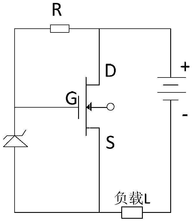
Figure 1 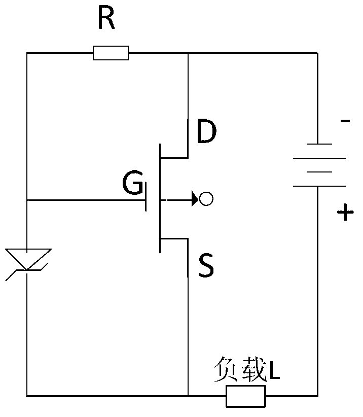
Figure 2 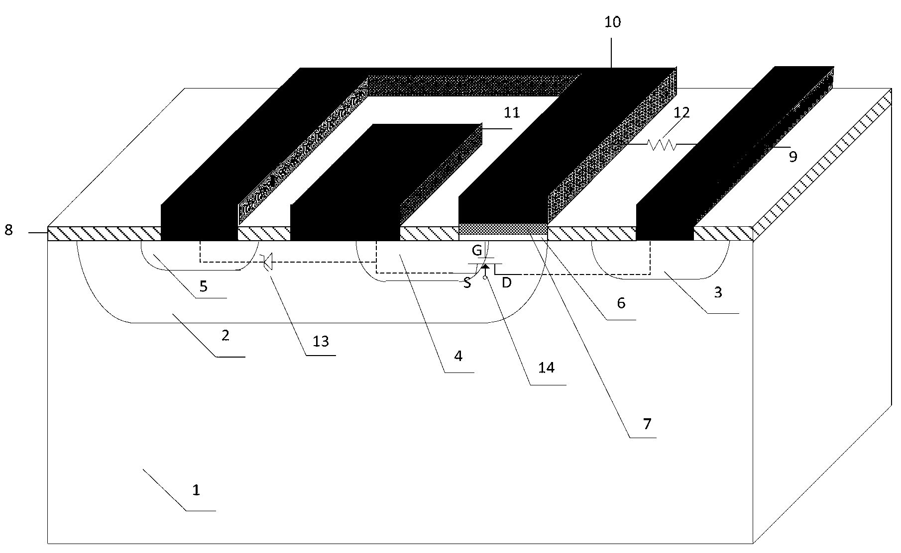
Figure 3
Abstract
Description
technical field
[0001] The invention belongs to the technical field of semiconductor devices and relates to constant current driving technology. Background technique
[0002] A constant current device is a device that can provide a constant current to the load, and it can keep the output current constant when the external power supply fluctuates and the impedance characteristics change. The constant current device has a development history of nearly 50 years. From the early electric vacuum device, the constant current tube, it has developed into a semiconductor constant current diode and a constant current triode, and now it has entered the integrated current Four-terminal adjustable constant current device, high-voltage constant current device, constant current type integrated temperature sensor) in a new era of comprehensive development. Semiconductor constant current devices are roughly divided into the following three types:
[0003] (1) Transistor constant current dev...
Examples
Embodiment 1
[0018] A semiconductor linear constant current device, such as image 3 As shown, it includes an N-type substrate 1, a P-type well region 2, a first N+ region 3, a second N+ region 4, and a third N+ region 5; wherein the P-type well region 2 and the first N+ region 3 are located on the N-type substrate bottom 1 top, and the P-type well region 2 and the first N+ region 3 are isolated from each other; the second N+ region 4 and the third N+ region 5 are located in the P-type well region 2 and are isolated from each other; the second N+ region 4 is located in the first N+ Between the region 3 and the third N+ region 5; the surface of the first N+ region 3 is connected to the first metal electrode 9; part of the second N+ region 4 and the P-type well region between the first N+ region 3 and the second N+ region 4 The surface of the gate oxide layer 2 has a gate oxide layer 6, the surface of the gate oxide layer 6 is a polysilicon gate electrode 7, and the surface of the polysilicon...
Embodiment 2
[0020] A semiconductor linear constant current device, such as image 3 As shown, it includes a P-type substrate 1, an N-type well region 2, a first P+ region 3, a second P+ region 4, and a third P+ region 5; wherein the N-type well region 2 and the first P+ region 3 are located on the P-type substrate bottom 1 top, and the N-type well region 2 and the first P+ region 3 are isolated from each other; the second P+ region 4 and the third P+ region 5 are located in the N-type well region 2 and are isolated from each other; the second P+ region 4 is located in the first P+ Between the region 3 and the third P+ region 5; the surface of the first P+ region 3 is connected to the first metal electrode 9; part of the second P+ region 4 and the N-type well region between the first P+ region 3 and the second P+ region 4 The surface of the gate oxide layer 2 has a gate oxide layer 6, the surface of the gate oxide layer 6 is a polysilicon gate electrode 7, and the surface of the polysilicon...