
PCB (printed circuit board) and electronic device
A technology for electronic devices and conductive layers, applied in the field of electronics, can solve problems such as peeling off and easy blistering of solder resist layers, and achieve the effects of preventing blistering, uniform heat dissipation, and reduced thermal expansion and cold shrinkage deformation rate
Patent Information
- Authority / Receiving Office
- CN · China
- Patent Type
- Applications(China)
- Current Assignee / Owner
- Publication Date
- 2013-05-01
- Estimated Expiration
- Not applicable · inactive patent
Smart Images

Figure 1 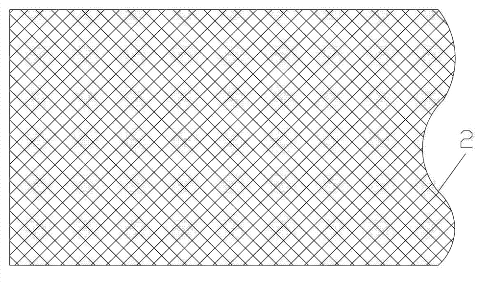
Figure 2 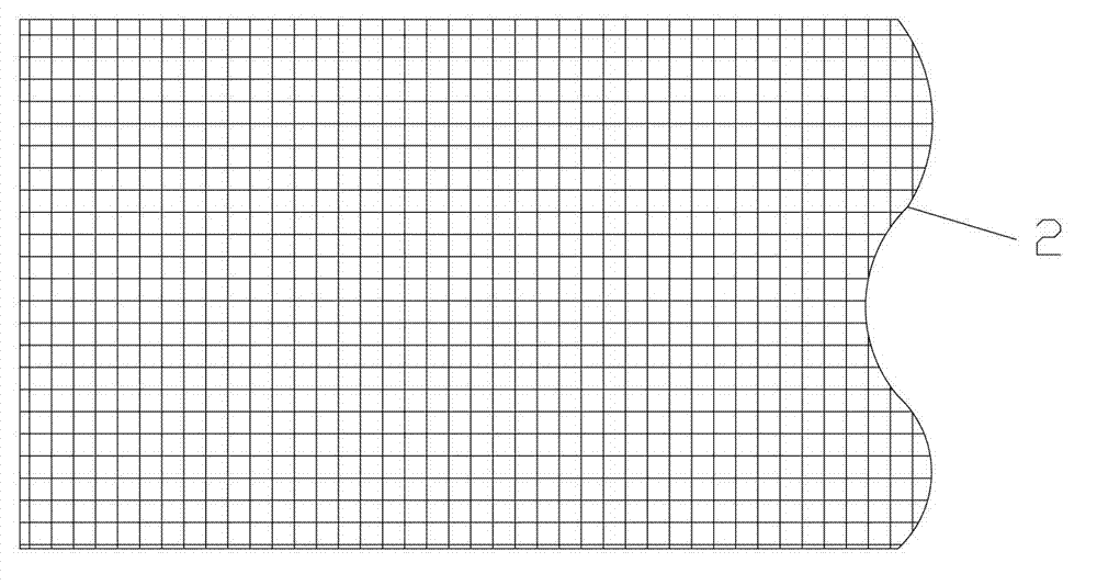
Figure 3
Abstract
Description
technical field
[0001] The invention belongs to the field of electronic technology, and in particular relates to a PCB and an electronic device. Background technique
[0002] When the PCB (Printed Circuit Board, printed circuit board, referred to as hard board) board with plug-in components passes through the wave soldering furnace, the soldering surface of the PCB board needs to be in contact with the boiling tin pick in the tin furnace to reach the component pins. The purpose of tinning. Due to the high boiling point of the tin pick, during the wave soldering process, when the PCB surface is in contact with the tin pick, the surface of the PCB will be heated sharply. Layers are blistered or peeled off. Contents of the invention
[0003] The purpose of the embodiments of the present invention is to provide a PCB, aiming to solve the problem that the solder resist layer of the existing PCB is easy to bubble and fall off after being reheated.
[0004] The embodiment of t...
Examples
Embodiment Construction
[0010] In order to make the object, technical solution and advantages of the present invention clearer, the present invention will be further described in detail below in conjunction with the accompanying drawings and embodiments. It should be understood that the specific embodiments described here are only used to explain the present invention, not to limit the present invention.
[0011] In the embodiment of the present invention, the conductive layer is set in a grid shape to reduce the actual heating area of the conductive layer. When the PCB passes through the furnace, the conductive layer actually receives less heat, and the heat is relatively dispersed, so that the heat dissipation is uniform and rapid, and the entire conductive layer heats up. The expansion and contraction deformation rate is greatly reduced, thereby preventing the solder mask layer from bubbling and falling off after the PCB goes through the furnace, and improving the reliability of the PCB and elect...