
Semiconductor packaging structure and heat dissipation member thereof
A technology of packaging structure and heat dissipation parts, which is applied in the direction of semiconductor devices, semiconductor/solid-state device parts, electric solid-state devices, etc. It can solve the problem of glue overflow in the central upper tip hole 421, uneven pressure in the mold, poor glue filling efficiency, etc. problems, to achieve the effect of suppressing glue overflow and avoiding glue overflow problems
Patent Information
- Authority / Receiving Office
- CN · China
- Patent Type
- Applications(China)
- Current Assignee / Owner
- Publication Date
- 2014-02-19
Smart Images
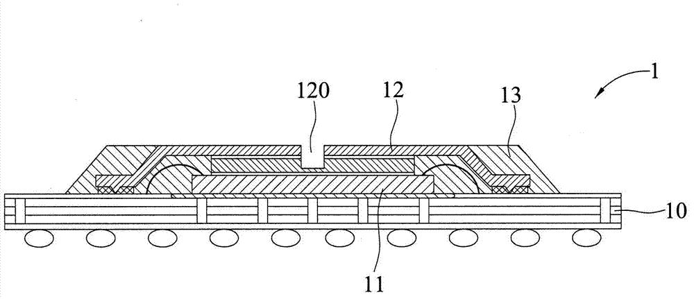
Figure 1 
Figure 2 
Figure 3
Abstract
Description
technical field
[0001] The invention relates to a semiconductor package structure, in particular to a semiconductor package structure with a heat sink and the heat sink. Background technique
[0002] In the heat dissipation technology of the current semiconductor packaging structure, heat sinks are often arranged outside the structure, so that the heat sink can be used as a heat dissipation path by contacting the heat sink with air, such as figure 1 The semiconductor packaging structure 1 shown has a packaging substrate 10, a semiconductor component 11 disposed on the packaging substrate 10, a heat sink 12 disposed on the packaging substrate 10 to cover the semiconductor component 11, and covering the semiconductor component 11. The encapsulant 13 on the sides of the semiconductor component 11 and the heat sink 12 . Wherein, the heat sink 12 has a central through hole 120 , so that the encapsulant 13 can be filled into the inner side of the heat sink 12 through the central ...
Examples
Embodiment Construction
[0080] The implementation of the present invention will be described below through specific examples, and those skilled in the art can easily understand other advantages and effects of the present invention from the content disclosed in this specification.
[0081] It should be noted that the structures, proportions, sizes, etc. shown in the drawings attached to this specification are only used to match the content disclosed in the specification for the understanding and reading of those skilled in the art, and are not intended to limit the implementation of the present invention. Limiting conditions, so there is no technical substantive meaning, any modification of structure, change of proportional relationship or adjustment of size, without affecting the effect and purpose of the present invention, should still fall within the scope of the present invention. The disclosed technical content must be within the scope covered. At the same time, terms such as "upper", "lower", "f...