
A High Voltage Super Junction Termination Structure
A junction terminal and terminal technology, applied in the field of high-voltage superjunction terminal structure, can solve the problems of increasing chip production cost, poor electric field uniformity, and increasing chip area, so as to reduce ion pollution and charge accumulation, and avoid electric field concentration effect. , the effect of preventing charge imbalance
Patent Information
- Authority / Receiving Office
- CN · China
- Patent Type
- Patents(China)
- Current Assignee / Owner
- Publication Date
- 2016-08-17
Smart Images
Figure 1 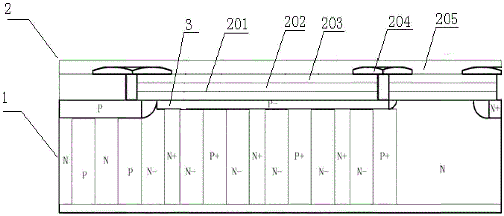
Figure 2 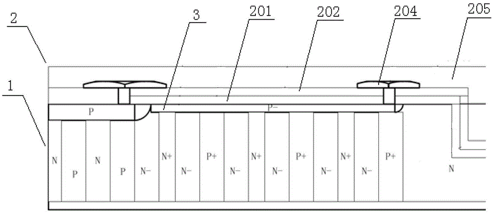
Figure 3
Abstract
Description
technical field
[0001] The invention relates to the field of manufacturing voltage-controlled power devices, in particular to a high-voltage super-junction terminal structure. Background technique
[0002] The ability of a device to block high voltage mainly depends on the reverse bias breakdown voltage of a specific PN junction in the device structure. In power devices, due to the influence of PN junction bending or surface non-ideal factors at the termination of the PN junction, the reverse bias breakdown voltage of the PN junction is limited to occur near the surface or in the local area of the junction bending relative to the parallel plane junction in the body. breakdown phenomenon. The junction terminal is a special structure specially designed to reduce the local electric field, improve the surface breakdown voltage and reliability, and make the actual breakdown voltage of the device closer to the ideal value of the parallel plane junction. In vertical conduction ...
Examples
Embodiment Construction
[0027] see figure 2 , the present invention provides a high-voltage super junction terminal structure, including a super junction region 1 composed of P+, N-, N+ columns distributed at intervals and a terminal surface structure 2 with a metal field plate and a SIPOS field plate, the super junction region 1 There is a layer of P-layer 3 between the terminal surface structure 2, and the surface of the terminal surface structure 2 silicon wafer is sequentially deposited with a high-resistance SIPOS layer 201, SiO 2 layer 202 , low-resistance SIPOS layer 203 , metal field plate 204 and nitrogen-doped SIPOS layer 205 .
[0028] see image 3 , a high-voltage super-junction terminal structure provided by an embodiment of the present invention, including a super-junction region 1 composed of P+, N-, N+ columns distributed at intervals and a terminal surface structure 2 with a metal field plate and a SIPOS field plate, the super-junction There is a layer of P-layer 3 between the are...