
A LED module light source
A technology of LED modules and LED chips, which is applied in the direction of electric light sources, semiconductor devices, lighting and heating equipment, etc., can solve problems such as fracture, low mechanical strength of bonding wires, internal stress damage of packaging colloid, etc., to eliminate internal stress, Excellent light extraction effect, avoiding shear stress and elastic modulus effect
Patent Information
- Authority / Receiving Office
- CN · China
- Patent Type
- Patents(China)
- Current Assignee / Owner
- Publication Date
- 2018-01-23
Smart Images
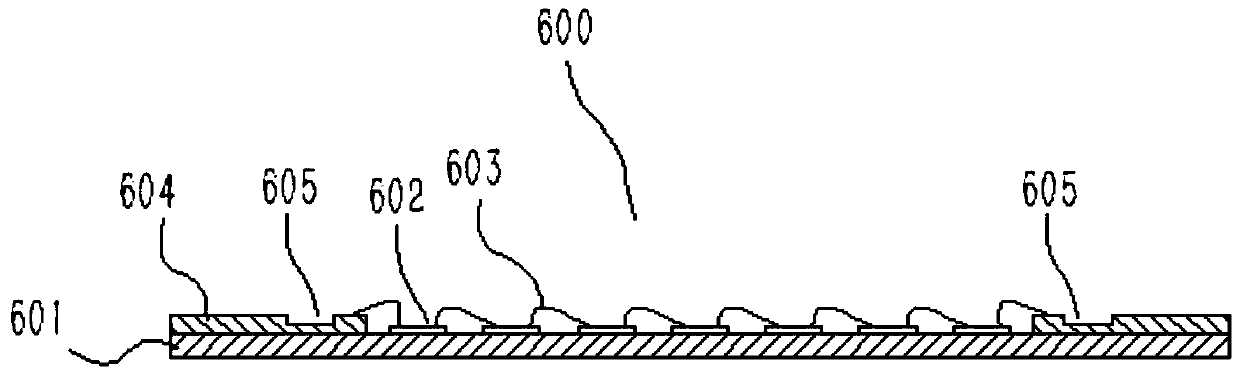
Figure 1 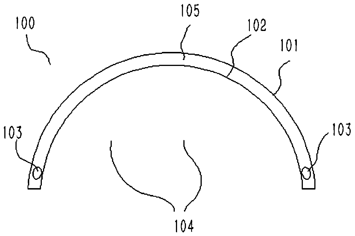
Figure 2 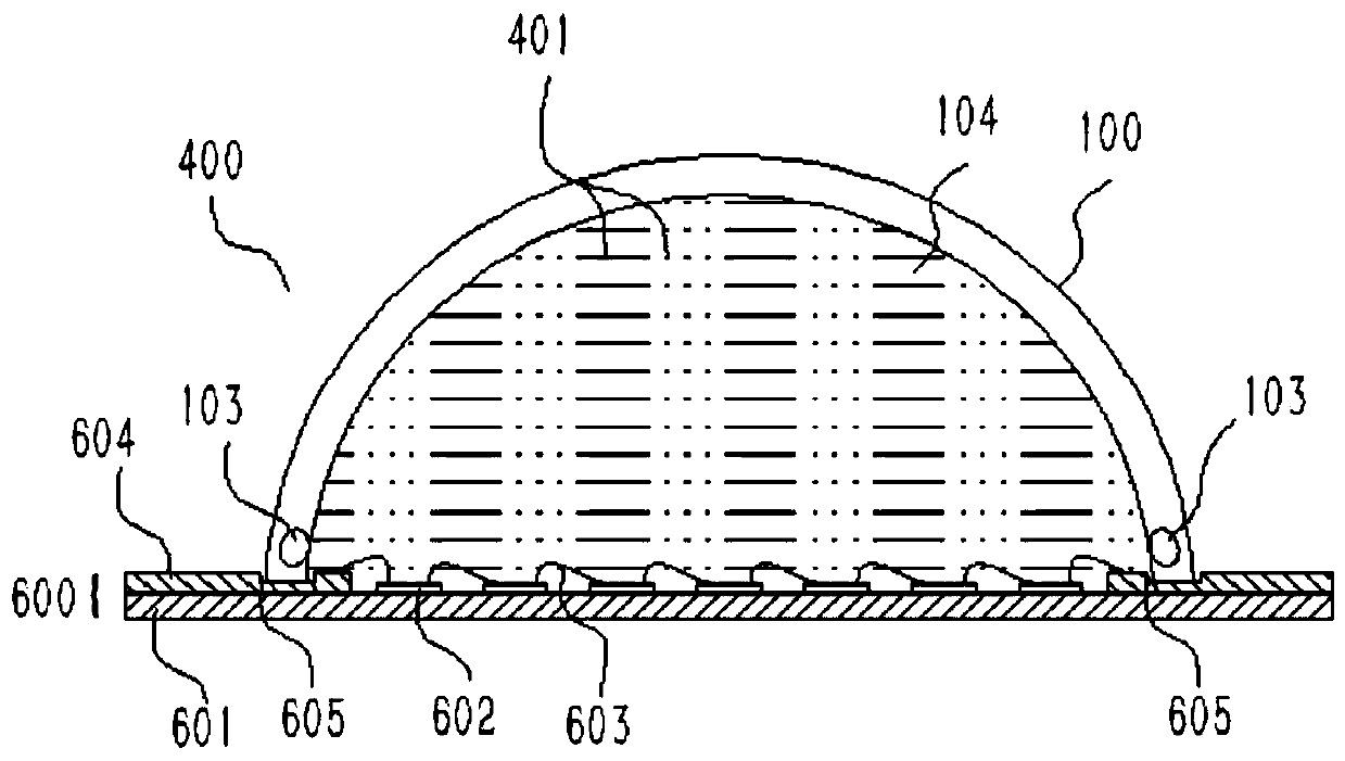
Figure 3
Abstract
Description
technical field
[0001] The invention relates to the technical field of LEDs, in particular to an LED module light source. Background technique
[0002] LED integrated module packaging light source is very popular in the fields of home lighting, commercial lighting, venues, and industrial and mining lighting. Integrated packaging has always played an important part of the LED lighting device market due to its excellent light quality, excellent light efficiency performance, good optical design latitude and excellent cost performance.
[0003] The general form of the LED integrated module light source is: metal, ceramic or other materials are used as the substrate, and a front-mounted or flip-chip LED chip is arranged on it. The chip area is surrounded by walls, and fluorescent conversion materials are coated in it.
[0004] Among them, the integrated module light source using flip-chip LED chips only occupies a small share in the market due to the high threshold of flip-chip ...
Examples
Embodiment 1
[0040] like Figure 2-4 As shown, the lens 100 is installed on the base 600 , and the opening edge of the lens 100 is butted and glued to the installation groove 605 of the base 600 .
[0041] The lens 100 includes a filling cavity 104 , the filling cavity 104 forms a closed space with the substrate 601 , and the first filler 401 is filled in the closed space. The first filler 401 is a colorless, transparent non-solid substance, and is non-conductive, thereby avoiding the shear stress and elastic modulus in the traditional solid potting glue, and completely eliminating the thermal loss caused by different packaging materials. The combination acts on the internal stress of the bonding wire, which greatly improves the long-term reliability of the bonding wire, thereby reducing the harsh requirements of the reliability of the package on the material system and packaging technology. The LED chip 602 and the bonding wire 603 are located in the enclosed space.
[0042] The lens 10...
Embodiment 2
[0053] The technical scheme of this embodiment and embodiment 1 is basically the same, and its difference mainly lies in:
[0054] The structure of the lens 200 of this embodiment is different from that of the lens 100 in Embodiment 1, wherein, as Figure 5 As shown, the inner surface 202 and the outer surface 201 of the lens body 205 in this embodiment are curved surfaces, and its cross-sectional view is wavy.
Embodiment 3
[0056] The technical scheme of this embodiment and embodiment 1 is basically the same, and its difference mainly lies in:
[0057] The structure of the lens 300 in this embodiment is different from that of the lens 100 in Embodiment 1 and the lens 200 in Embodiment 2, wherein, as Figure 6 As shown, the inner surface 302 of the lens body 305 in this embodiment is a curved surface, specifically as Figure 6 It is a curved surface, and the outer surface 301 is a serrated plane.
[0058] It should be noted that the structure of the lens of the present invention includes but not limited to the three structures described in Embodiments 1, 2 and 3.