
Frequency modulation type constant-voltage output power supply based on high-voltage absorption circuit
A technology of absorbing circuit and constant voltage output, applied in the field of electronics, can solve the problems of unstable output voltage, low power supply stability, easy to be affected by mains fluctuations, etc., to achieve the effect of improving safety performance, stable voltage and frequency, and good power supply
Patent Information
- Authority / Receiving Office
- CN · China
- Patent Type
- Applications(China)
- Current Assignee / Owner
- Publication Date
- 2016-10-12
- Estimated Expiration
- Not applicable · inactive patent
Smart Images
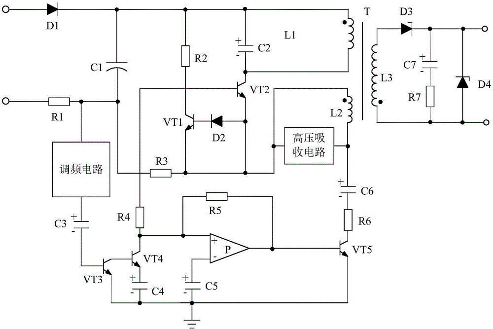
Figure 1 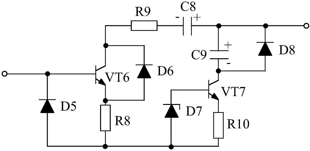
Figure 2 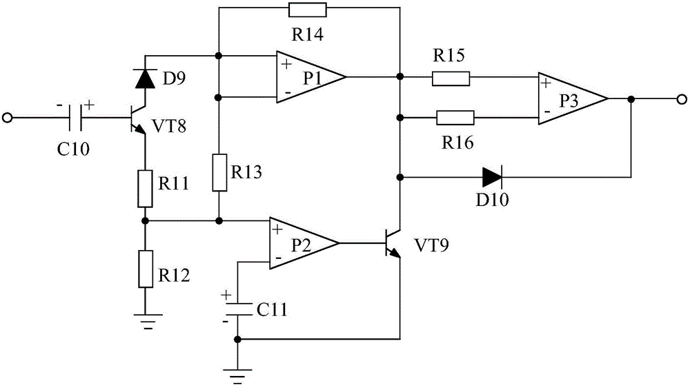
Figure 3
Abstract
Description
Technical field
[0001] The invention relates to the field of electronics, in particular to a frequency modulation type constant voltage output power supply based on a high voltage absorption circuit. Background technique
[0002] With the rapid development of electronic technology, there are more and more types of electronic equipment, which brings great pleasure to people's lives. Any electronic device is inseparable from a reliable power source. At present, the functions of electronic devices are becoming more and more diversified, and their requirements for power sources are getting higher and higher. However, current power supplies have low stability and are easily affected by mains fluctuations, resulting in unstable output voltage, which seriously affects the service life of electronic devices. Summary of the invention
[0003] The purpose of the present invention is to solve the defect of low stability of the current power supply and provide a frequency-modulated constant-...
Examples
Embodiment
[0019] Such as figure 1 As shown, the present invention mainly consists of a transformer T, a diode D1, a transistor VT5, and a base trigger circuit respectively connected to the primary inductor coil L1 and the primary inductor coil L2 of the transformer T, one end is connected to the base trigger circuit, and the other One end and the P pole of the diode D1 together form the input resistor R1, the positive pole is connected to the non-identical end of the secondary inductor L2 of the transformer T, and the negative pole is connected to the collector of the transistor VT5 through the resistor R6. The capacitor C6 is respectively connected with The sampling circuit connected to the triode VT5 and the base trigger circuit, and the frequency modulation circuit connected to the sampling circuit and the base trigger circuit respectively, are connected in series to the high voltage between the same-named end and the non-same-named end of the primary inductor coil L2 of the transformer...