
Integrated semiconductor bridge transduction element
A technology of transducing components and semiconductors, which is applied in the direction of weapon accessories, blasting barrels, offensive equipment, etc., can solve problems such as interference, electromagnetic damage, and heat accumulation damage of electrical explosives, and achieve strong anti-electromagnetic interference performance and large design margin , the effect of improving reliability
Patent Information
- Authority / Receiving Office
- CN · China
- Patent Type
- Applications(China)
- Current Assignee / Owner
- Publication Date
- 2017-09-29
Smart Images
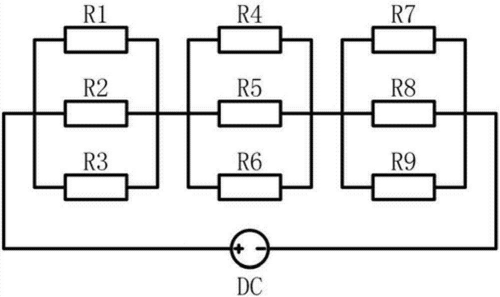
Figure 1 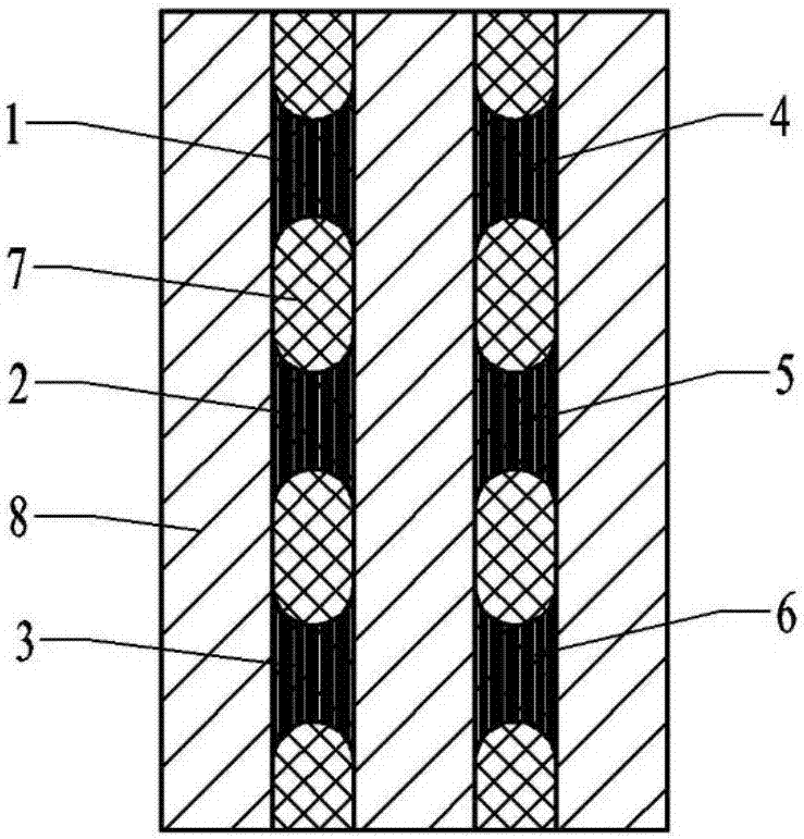
Figure 2 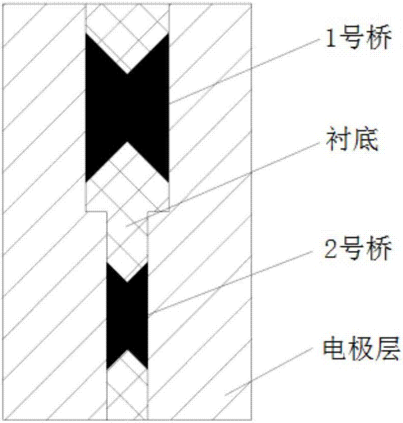
Figure 3
Abstract
Description
technical field
[0001] The invention belongs to the technical field of semiconductor bridge pyrotechnics, and in particular relates to an integrated semiconductor bridge transducing element. Background technique
[0002] Semiconductor bridge pyrotechnic products are widely used in ignition and detonation systems of weapon systems and civilian blasting equipment due to their excellent quality. At the same time, with the increasingly harsh electromagnetic environment, the requirements for the anti-electromagnetic environment capability of semiconductor bridge pyrotechnic products are also getting higher and higher. For example, for its safety, it is generally required to achieve 1.A.1W.5min insensitivity or higher insensitivity, and for its reliability, its reliability is generally required to be 0.995-0.9999 (confidence level 0.95). Existing semiconductor bridge chips have been difficult to resist external electromagnetic field energy interference in harsh electromagnetic en...
Examples
Embodiment
[0059] figure 1 It is the schematic diagram of the series-parallel circuit of the integrated semiconductor bridge. The integrated semiconductor bridge is designed according to the safety and reliability requirements of the ignition system. Parallel and series-parallel hybrid circuits,
[0060] combine figure 2 1, 2, 3, 4, 5 and 6 in the figure are respectively series-parallel semiconductor bridges formed by six semiconductor bridge regions, each having a different position, 7 is an electrode layer, and 8 is an insulating layer. The reinforcement of the electromagnetic environment interference energy is shared by the six bridges. When the ignition input energy is applied, the six bridges respectively convert and output six plasmas to ignite the pyrotechnic agent at their respective positions.
[0061] combine image 3 with Figure 4 , In the high insensitivity pyrotechnics integrated parallel semiconductor bridge, N bridges are formed into a parallel circuit, and the two b...