
Chip antenna apparatus and wireless communication apparatus
A technology of chip antenna and antenna part, which is applied in the direction of antenna grounding device, antenna support/installation device, antenna, etc., can solve the problem of stable operation of antenna device, achieve the effects of reducing sensitivity, ensuring radiation efficiency, and avoiding loss
Patent Information
- Authority / Receiving Office
- CN · China
- Patent Type
- Applications(China)
- Current Assignee / Owner
- Publication Date
- 2018-04-13
- Estimated Expiration
- Not applicable · inactive patent
Smart Images
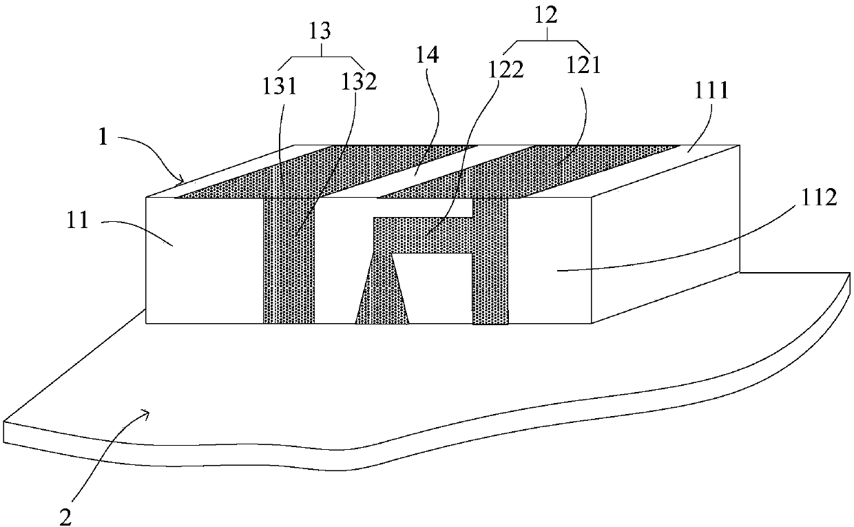
Figure 1 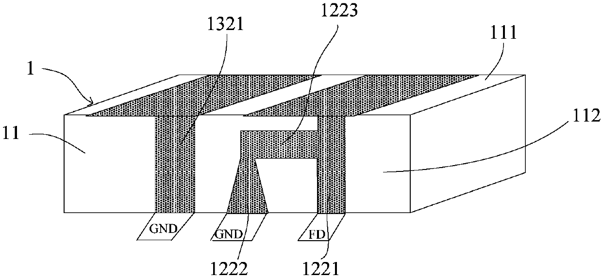
Figure 2 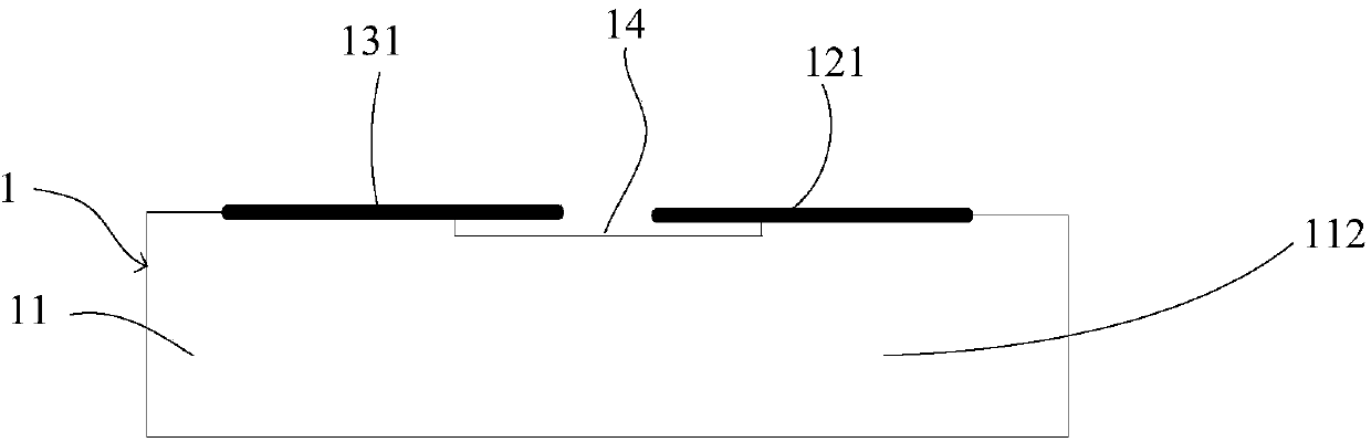
Figure 3
Abstract
Description
technical field
[0001] The invention relates to the field of wireless communication, in particular to a chip antenna device and wireless communication equipment. Background technique
[0002] In the field of wireless communication, for example, in wireless communication devices with wireless communication functions such as mobile phones (including smart phones), tablet PCs, and smart watches, one or more antenna devices are installed inside the wireless communication devices. The miniaturization of equipment has also continuously put forward requirements for the miniaturization and thinning of antenna devices. Therefore, chip antenna devices are widely used in the field of wireless communication at present. Chip antennas usually include a dielectric substrate and a radiating element and a parasitic element arranged on the surface of the dielectric substrate. The radiating element transmits and receives signals. Feed electromagnetically to match resonance to tune antenna ban...
Examples
Embodiment Construction
[0025] In order to make the object, technical solution and advantages of the present invention clearer, the present invention will be further described in detail below in conjunction with the accompanying drawings and embodiments. It should be understood that the specific embodiments described here are only used to explain the present invention, not to limit the present invention.
[0026] see figure 1 , figure 1 A schematic diagram of a wireless communication device according to the first embodiment of the present invention is shown, the wireless communication device includes a chip antenna device 1 and a circuit substrate 2, the chip antenna device 1 is arranged on the circuit substrate 2, and the circuit substrate 2 may be a PCB board . Wherein, the chip antenna device 1 includes a rectangular parallelepiped dielectric substrate 11 , and a first radiating element 12 and a second radiating element 13 disposed on the surface of the substrate 11 and spaced apart from each ot...