
Oscillator and chip
A technology of oscillator and comparator, which is applied in the direction of pulse generation, electrical components, and electric pulse generation. It can solve the problems of complex circuit design, increase of layout area, and increase of cost, so as to save chip area, reduce cost, and save circuit. Effects of Design Complexity
Patent Information
- Authority / Receiving Office
- CN · China
- Patent Type
- Applications(China)
- Current Assignee / Owner
- Publication Date
- 2019-04-05
- Estimated Expiration
- Not applicable · inactive patent
Smart Images
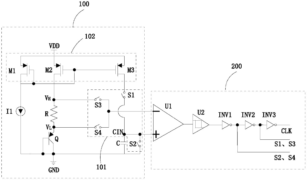
Figure 1 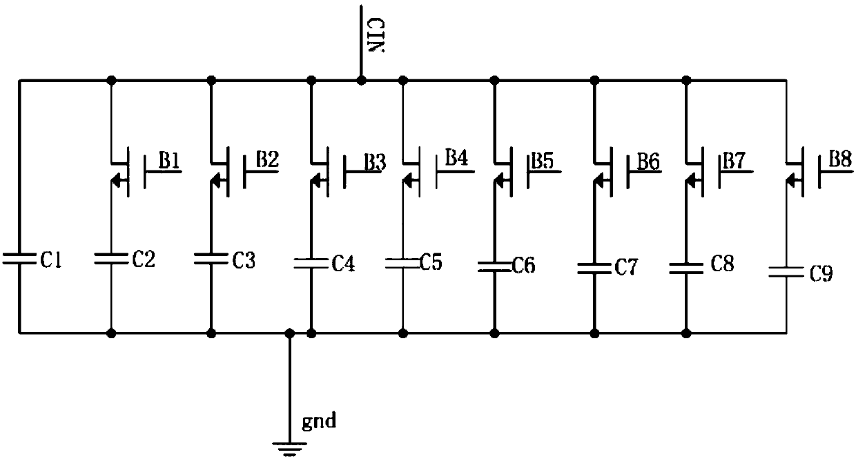
Figure 2 
Figure 3
Abstract
Description
technical field
[0001] The invention relates to the technical field of integrated circuit design, in particular to an oscillator and a chip thereof. Background technique
[0002] The Internet of Things and artificial intelligence are currently the hottest research directions in the world, and these researches are all based on chips. For smart chips, oscillators are indispensable.
[0003] Traditional oscillators generally require two comparators, a capacitor, and a set of bias circuits for charging and discharging the capacitor. A high threshold and a low threshold are respectively input to the two comparators. When the capacitor voltage is greater than the high threshold, a comparator Flip, control the discharge of the bias circuit, the capacitor voltage drops, when the capacitor voltage is less than the low threshold, another comparator flips, control the charge of the bias circuit, the voltage rises, and so on, output an oscillation signal. For example, the invention pat...
Examples
Embodiment Construction
[0021] The technical solutions in the present invention will be clearly and completely described below in conjunction with the drawings in the embodiments of the present invention. Obviously, the described embodiments are only part of the embodiments of the present invention, not all of them.
[0022] Such as figure 1 As shown, an oscillator includes a charging and discharging module 100 and a control module 200. The charging and discharging module 100 includes a capacitor C, a current source I1, a resistor R, a switch unit 101, a current mirror unit 102, and a transistor Q. The control The module 200 includes a comparator U1, a flip-flop U2, a first inverter INV1, a second inverter INV2, and a third inverter INV3,
[0023] The first end of the capacitor C is connected to the current source I1 through the switch unit 101, the second end of the capacitor C is grounded, and the voltage on the capacitor C is expressed as V CIN , the first end of the resistor R is connected to th...