
Array substrate, preparation method thereof, and display panel
An array substrate and area technology, which is applied in the fields of array substrates and their preparation, and display panels, can solve the problems of touch failure, inability to sense user touch signals, etc.
Patent Information
- Authority / Receiving Office
- CN · China
- Patent Type
- Applications(China)
- Current Assignee / Owner
- Publication Date
- 2019-06-07
Smart Images
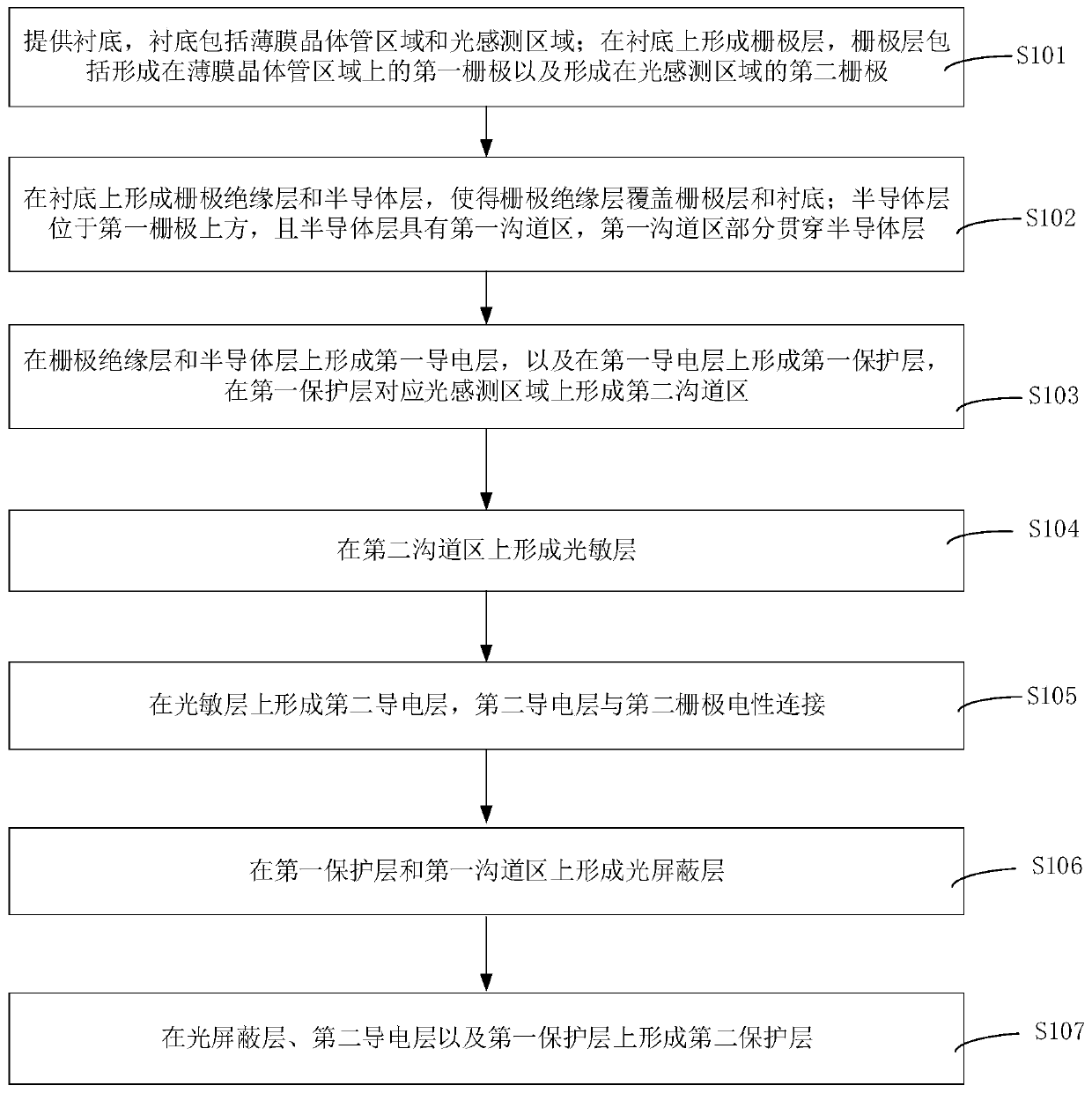
Figure 1 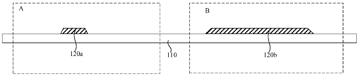
Figure 2 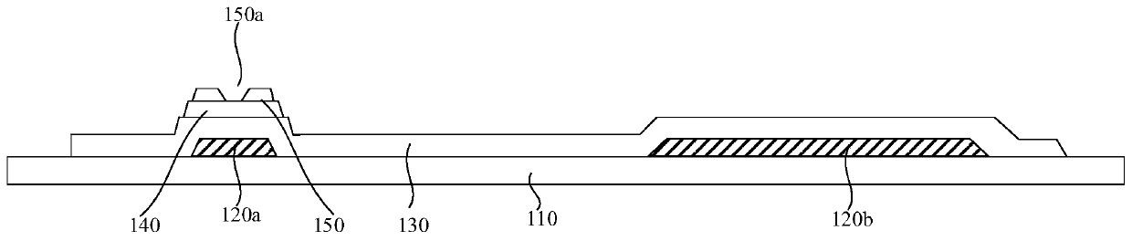
Figure 3
Abstract
Description
technical field
[0001] The present invention relates to the field of display technology, in particular to an array substrate, a preparation method thereof, and a display panel. Background technique
[0002] With the development of the display technology, it becomes a trend to combine the touch technology with the display panel, that is, the integration of the touch panel and the display panel. In an exemplary touch display panel, a PS (Photo Spacer, spacer) is formed on a color filter substrate, an ITO electrode is formed on the PS, and an ITO electrode is correspondingly formed on the array substrate. When a user's finger presses the color filter substrate, the indium tin oxide electrode on the spacer and the indium tin oxide electrode on the array substrate are contacted and conducted to transmit the touch signal. However, because touch often causes dislocation of the upper and lower substrates (color filter substrate and array substrate), the dislocation phenomenon makes...
Examples
Embodiment Construction
[0050]In order to facilitate the understanding of the present invention, the present invention will be described more fully below with reference to the associated drawings. Preferred embodiments of the invention are shown in the accompanying drawings. However, the present invention can be embodied in many different forms and is not limited to the embodiments described herein. On the contrary, these embodiments are provided to make the understanding of the disclosure of the present invention more thorough and comprehensive.
[0051] Unless otherwise defined, all technical and scientific terms used herein have the same meaning as commonly understood by one of ordinary skill in the technical field of the invention. The terminology used herein in the description of the present invention is only for the purpose of describing specific embodiments, and is not intended to limit the present invention.
[0052] see figure 1 , figure 1 It is a schematic flowchart of the method for pr...