
Error frequency modulation method for reducing THD (Total Harmonic Distortion) of single-phase photovoltaic grid-connected inverter
A modulation method and inverter technology, applied in photovoltaic power generation, harmonic reduction devices, single-network parallel feeding arrangements, etc., can solve the problems of not being used in practice, and cannot improve the output performance of the inverter, so as to improve the electric energy High quality, THD reduction, and excellent output performance
Patent Information
- Authority / Receiving Office
- CN · China
- Patent Type
- Applications(China)
- Current Assignee / Owner
- Publication Date
- 2019-10-22
Smart Images
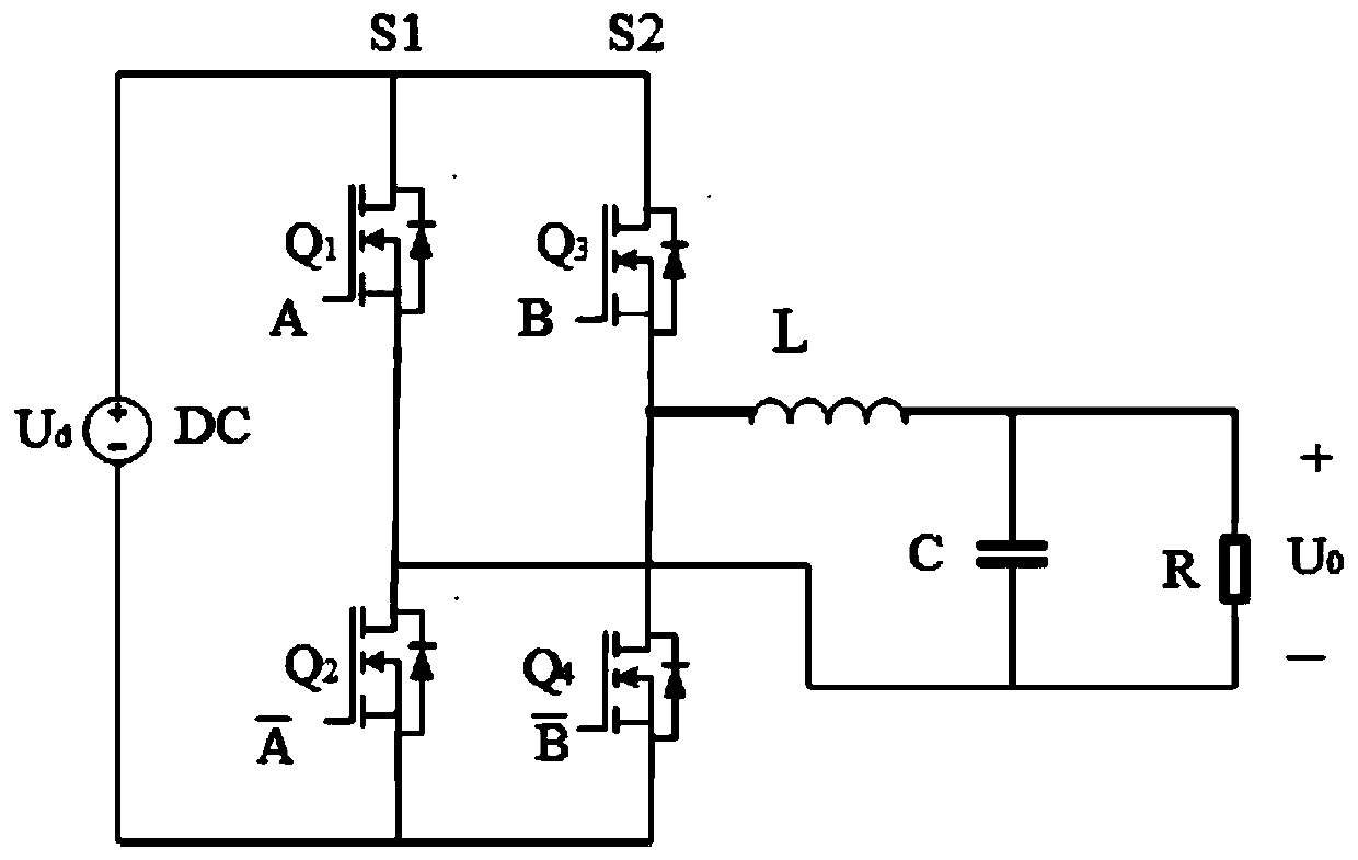
Figure 1 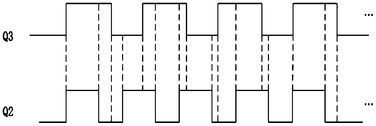
Figure 2 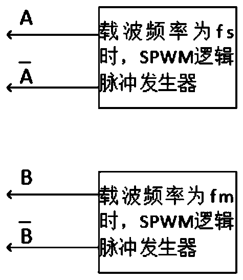
Figure 3
Abstract
Description
technical field
[0001] The invention relates to the technical field of single-phase photovoltaic grid connection, in particular to a frequency-staggering method for a single-phase inverter to reduce the THD (total harmonic distortion) of the inverter. Background technique
[0002] Photovoltaic grid-connection is one of the important applications of photovoltaic power generation. However, the harmonics generated by photovoltaic grid-connected inverters will pollute the grid. Reducing the THD generated by photovoltaic grid-connected devices can effectively reduce the pollution to the grid and increase the grid-connected power. quality.
[0003] The grid connection of large-scale photovoltaic power sources has led to the introduction of a large number of power electronic converters into the power system, so that a large number of nonlinear loads are also added to the power supply system, which will cause serious pollution to the power system and cause more serious power quality...
Examples
Embodiment Construction
[0027] In order to better understand the technical solution of the present invention, the present invention will be further described in detail below in conjunction with the accompanying drawings and embodiments.
[0028] The embodiment of the present invention provides a method for reducing THD through frequency shift technology, which is implemented for the existing single-phase inverter topology main circuit. The single-phase inverter topology main circuit includes a DC source, a first switch tube, a second switch tube, a third switch tube, a fourth switch tube, an output filter inductor, an output filter capacitor and a load.
[0029] Such as figure 1 As shown, the interleaved topology circuit includes a direct current source DC, a first switching tube Q 1 , the second switching tube Q 2 , the third switching tube Q 3 , the fourth switching tube Q 4 , Output filter inductor L, output filter capacitor C and load R. The four switch tubes are metal oxide semiconductor fi...