
Display panel, preparation method thereof and display device
A technology for display panels and preparation steps, which is applied in the directions of instruments, computing, optics, etc., can solve problems such as poor effect and low sensitivity of fingerprint recognition, and achieve the effect of improving display effect, ensuring sensitivity, and reducing interference electric field
Patent Information
- Authority / Receiving Office
- CN · China
- Patent Type
- Applications(China)
- Current Assignee / Owner
- Publication Date
- 2020-05-08
Smart Images
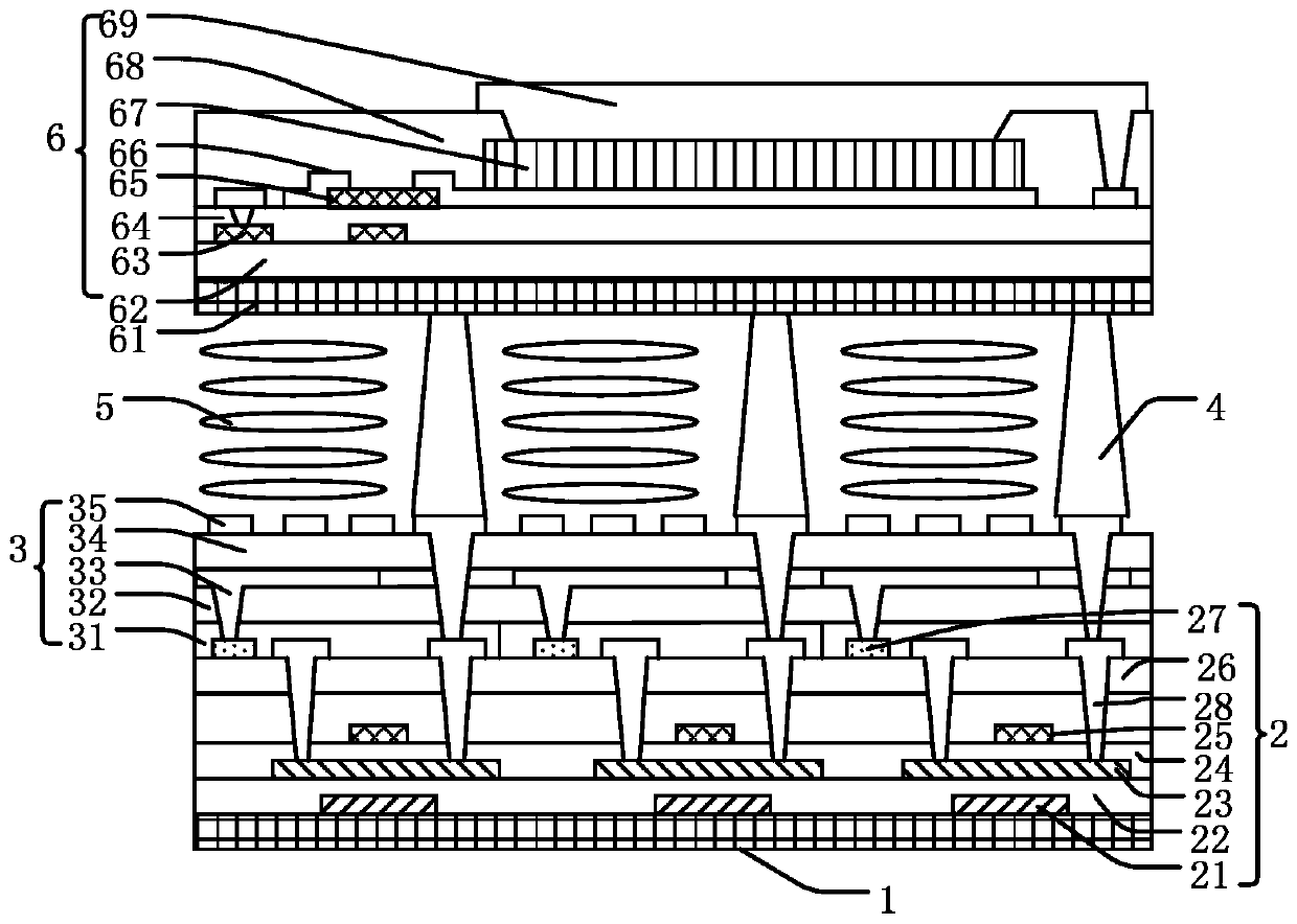
Figure 1 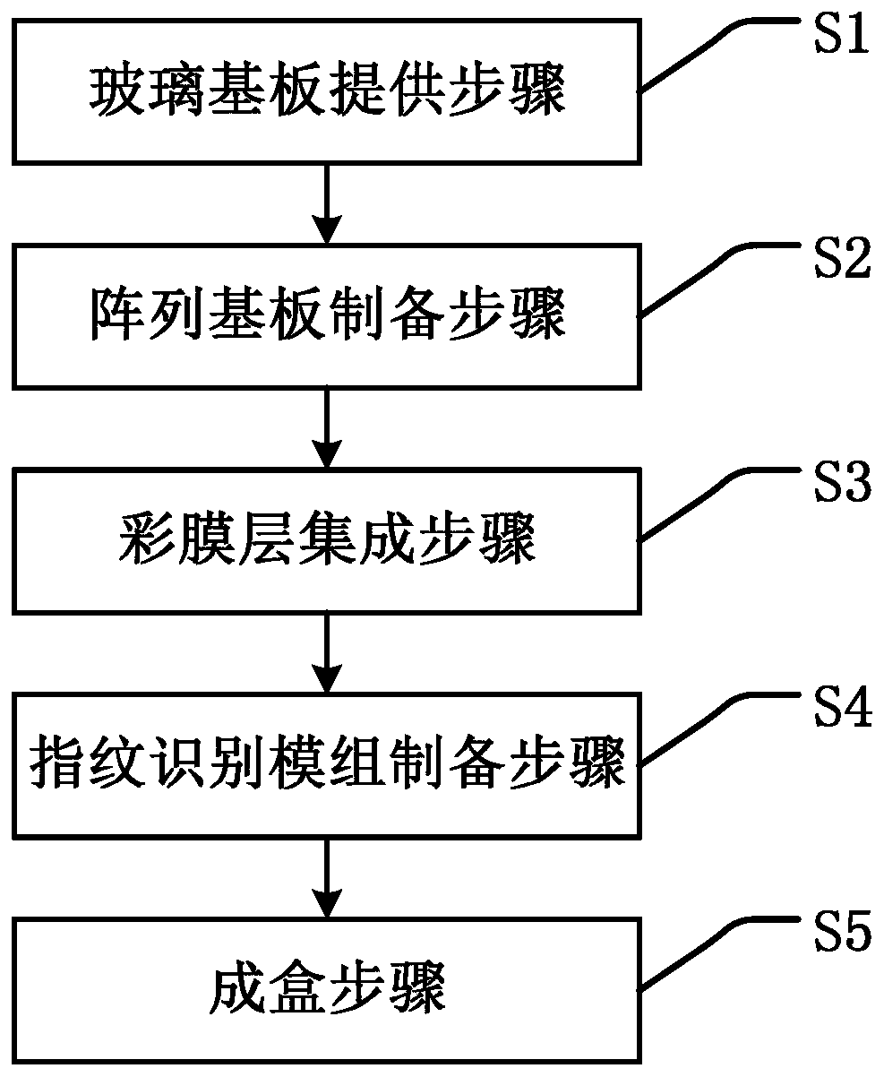
Figure 2 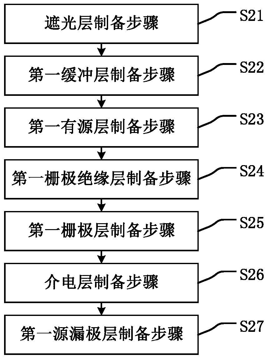
Figure 3
Abstract
Description
technical field
[0001] The present invention relates to the field of display, and in particular, to a display panel, a preparation method thereof, and a display device. Background technique
[0002] As a biometric identification method, fingerprint identification has attracted widespread attention recently, especially in mobile payment. People have also invented many methods of fingerprint identification, such as optical, capacitive, microwave, temperature and ultrasonic and many other methods. However, each approach has its advantages and disadvantages. For example, the traditional optical sensor method cannot achieve thin and light, especially under the requirement of high resolution, the traditional device is bulky and cannot be portable, so it is difficult to integrate into a device such as a mobile phone. Although other methods solve the problem of thinness and lightness, they cannot realize a large-area array, or cannot combine other functions, and the process is com...
Examples
Embodiment Construction
[0031] The technical solutions in the embodiments of the present application will be clearly and completely described below with reference to the accompanying drawings in the embodiments of the present application. Obviously, the described embodiments are only a part of the embodiments of the present application, but not all of the embodiments. Based on the embodiments in the present application, all other embodiments obtained by those skilled in the art without creative work fall within the protection scope of the present application.
[0032] In the description of this application, it should be understood that the terms "center", "longitudinal", "lateral", "length", "width", "thickness", "upper", "lower", "front", " rear, left, right, vertical, horizontal, top, bottom, inside, outside, clockwise, counterclockwise, etc., or The positional relationship is based on the orientation or positional relationship shown in the accompanying drawings, which is only for the convenience ...