
Display device, array substrate and method for manufacturing array substrate
A technology of an array substrate and a manufacturing method, applied in the field of display devices, can solve the problems of pollution, poor SiNx film quality and poor isolation effect, and increasing maintenance costs.
Patent Information
- Authority / Receiving Office
- CN · China
- Patent Type
- Patents(China)
- Current Assignee / Owner
- Publication Date
- 2021-04-23
Smart Images
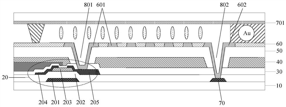
Figure 1 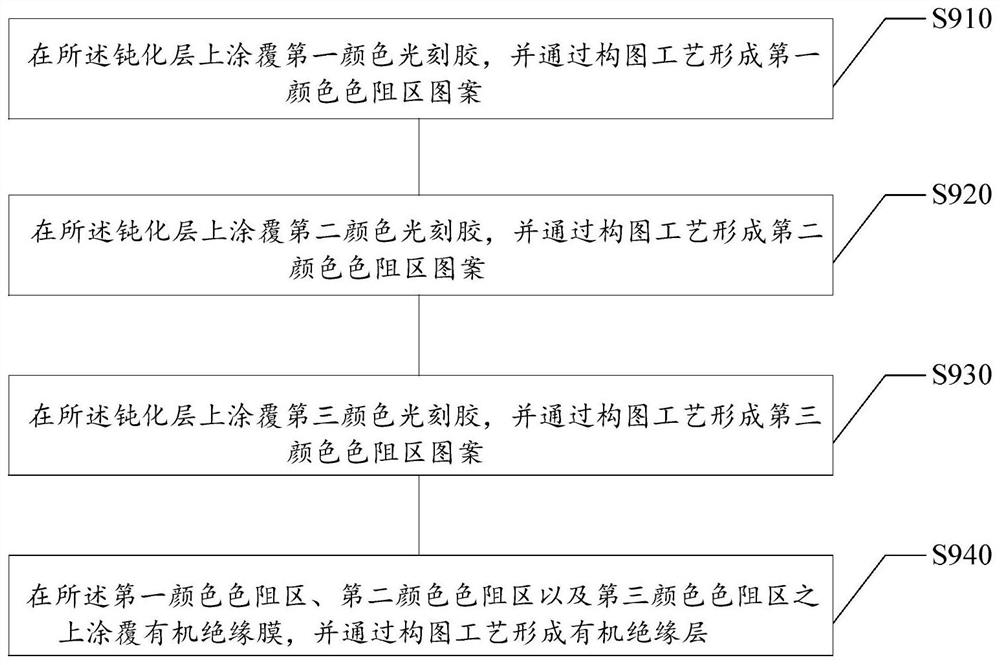
Figure 2 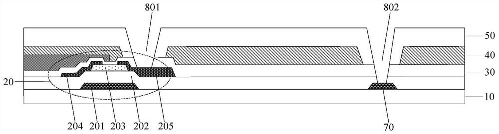
Figure 3
Abstract
Description
technical field
[0001] The present disclosure relates to the technical field of liquid crystal display, and in particular, to an array substrate, a manufacturing method of the array substrate, and a display device including the array substrate. Background technique
[0002] PSVA (Polmer Stabilized Vertically Aligned, Polymer Stabilized Vertically Aligned) mode has become the mainstream technology of LCD TVs because of its good dark state performance, high contrast, and small light leakage on curved surfaces. In order to overcome the VA (Vertivally Alignment, vertical alignment mode) viewing angle problem, people adopt designs such as 4 chips and 8 chips, which greatly improve the performance under large viewing angles. At present, PSVA has excellent dark state and curved surface light leakage performance. By designing the pixel electrode into a comb-like shape, 8 chips can be realized, which can make up for the light leakage and color distortion problems of side viewing angl...
Examples
Embodiment Construction
[0043] Example embodiments will now be described more fully with reference to the accompanying drawings. Example embodiments may, however, be embodied in many forms and should not be construed as limited to the examples set forth herein; rather, these embodiments are provided so that this disclosure will be thorough and complete and will fully convey the concept of example embodiments to those skilled in the art. The described features, structures, or characteristics may be combined in any suitable manner in one or more embodiments. In the following description, numerous specific details are provided in order to give a thorough understanding of embodiments of the present disclosure. However, those skilled in the art will appreciate that the technical solutions of the present disclosure may be practiced without one or more of the specific details being omitted, or other methods, components, devices, steps, etc. may be adopted. In other instances, well-known technical solution...