

Semiconductor device and manufacturing method thereof
A technology of semiconductors and wide-bandgap semiconductors, which is applied in semiconductor/solid-state device manufacturing, semiconductor devices, electrical components, etc., and can solve problems such as difficulty in reducing the size of unit cells
Patent Information
- Authority / Receiving Office
- CN · China
- Current Assignee / Owner
- Publication Date
- 2021-07-13
Smart Images
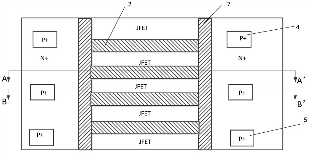
Figure 1 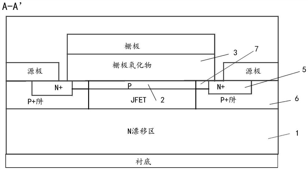
Figure 2 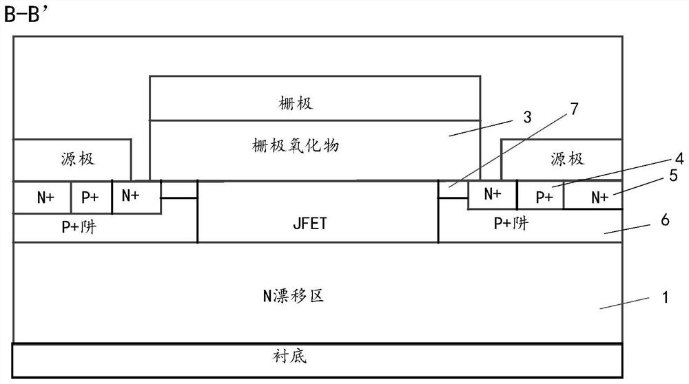
Figure 3
Abstract
Description
technical field
[0001] The invention relates to the field of transistor structures, in particular to a semiconductor device and a manufacturing method thereof. Background technique
[0002] For semiconductor devices, one potential problem is the presence of high electric fields at the gate oxide of the junction field effect (JFET) region of the device. The JFET region is typically the active part of the N-type drift region, which may include N-type dopants, and is located between the two P-type wells. The JFET region may refer to a region in contact with a channel region that reaches the surface of the P-type well by applying a gate voltage. The JFET region together with the N+ source region, the channel region, the N-type drift region, the substrate and the drain electrode constitute a conduction path for electrons. Under operating conditions where a high bias voltage is applied to the drain (close to the operating maximum) and the gate is held close to ground potential, ...
Examples
Embodiment Construction
[0026] In order to make the purpose, technical solutions and advantages of the embodiments of the present invention clearer, the technical solutions in the embodiments of the present invention will be clearly and completely described below in conjunction with the drawings in the embodiments of the present invention. Obviously, the described embodiments It is a part of embodiments of the present invention, but not all embodiments. Based on the embodiments of the present invention, all other embodiments obtained by those skilled in the art without creative efforts fall within the protection scope of the present invention.
[0027] This invention may be embodied in many different forms and should not be construed as limited to the embodiments set forth herein. Rather, these embodiments are provided so that this disclosure will be thorough and complete and will fully convey the concept of the invention to those skilled in the art, and the present invention will only be defined by ...