
Semiconductor component, composite coating forming method and plasma reaction device
A plasma and composite coating technology, which is applied in semiconductor/solid-state device manufacturing, electrical components, discharge tubes, etc., can solve the problems of coating protection function affecting plasma corrosion resistance and low production efficiency of plasma etching, etc. Achieve the effects of reducing etching costs, reducing the risk of failure, and improving efficiency
Patent Information
- Authority / Receiving Office
- CN · China
- Patent Type
- Applications(China)
- Current Assignee / Owner
- Publication Date
- 2022-02-22
Smart Images
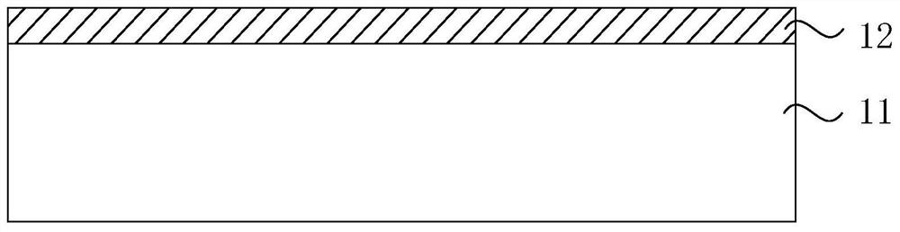
Figure 1 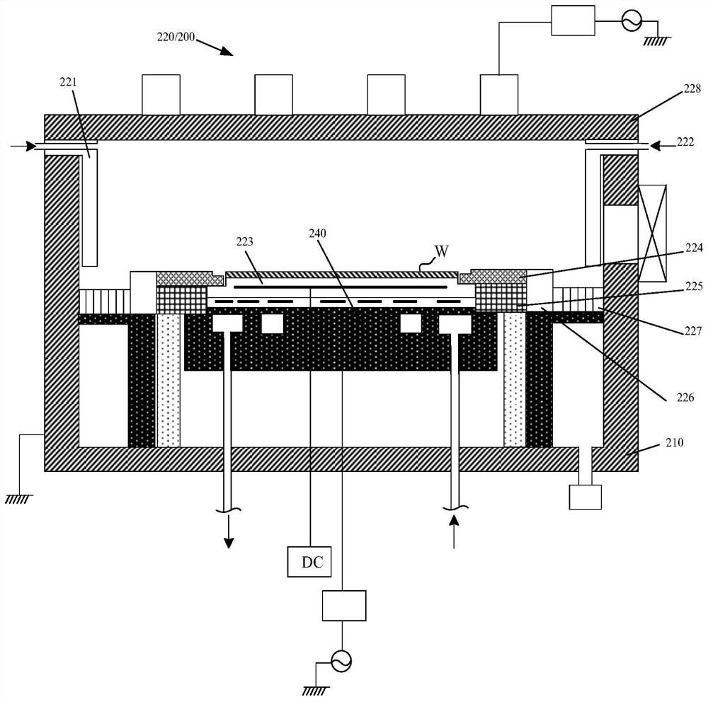
Figure 2 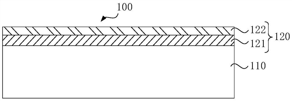
Figure 3
Abstract
Description
technical field
[0001] The invention relates to the technical field of plasma etching, in particular to a semiconductor component, a composite coating forming method and a plasma reaction device. Background technique
[0002] In the manufacturing process of semiconductor devices, plasma etching is a key process for processing wafers into design patterns. In a typical plasma etching process, a process gas is excited by a radio frequency (Radio Frequency, RF) to form a plasma. After passing through the electric field between the upper electrode and the lower electrode, these plasmas physically bombard and chemically react with the wafer surface, thereby etching a wafer with a specific structure.
[0003] During the plasma etching process, physical bombardment and chemical reaction will also act on all parts in the etching chamber that are in contact with the plasma, causing corrosion. For the workpiece in the etching chamber, some plasma corrosion-resistant coatings are usua...
Examples
Embodiment Construction
[0039] In the description of the present invention, the terms "first" and "second" are used for descriptive purposes only, and cannot be understood as indicating relative importance, or implicitly indicating the quantity of indicated technical features. Therefore, unless otherwise specified, the features defined as "first" and "second" may explicitly or implicitly include one or more of these features; "plurality" means two or more. The term "comprising" and any variations thereof mean non-exclusive inclusion, possible presence or addition of one or more other features, integers, steps, operations, units, components and / or combinations thereof. It should be understood that the terminology used and specific structural and functional details disclosed herein are merely representative for describing specific embodiments, but the invention may be embodied in many alternative forms and should not be construed as merely Be limited by the examples set forth herein.
[0040] Also, Ce...