
Copper reflow process
a technology of copper reflow and copper, which is applied in the direction of semiconductor/solid-state device manufacturing, basic electric elements, electric apparatus, etc., can solve the problems of aluminum resistance becoming non-negligible, resistance-capacitance (rc) time delay of the circuit, and the deficiency of aluminum and its allows becoming limiting factors in achieving superior performance. , to achieve the effect of improving the adhesion, reducing variability, and better modeling a process
Patent Information
- Authority / Receiving Office
- US · United States
- Patent Type
- Applications(United States)
- Current Assignee / Owner
- Publication Date
- 2003-07-24
- Estimated Expiration
- Not applicable · inactive patent
Smart Images
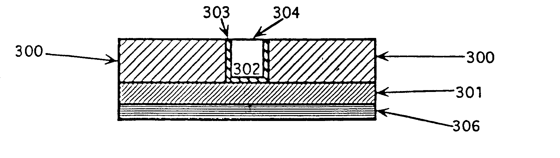
Figure 1 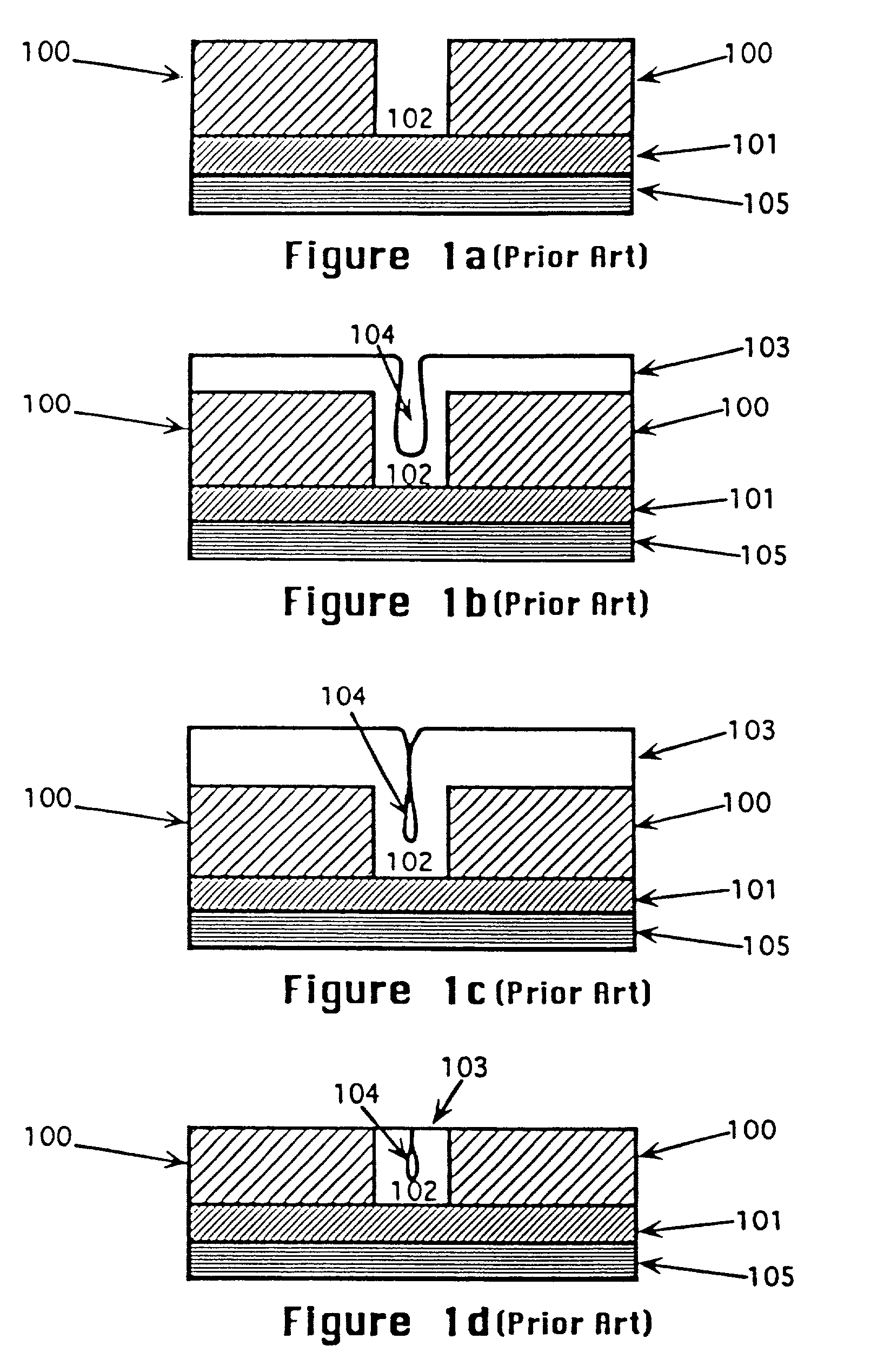
Figure 2 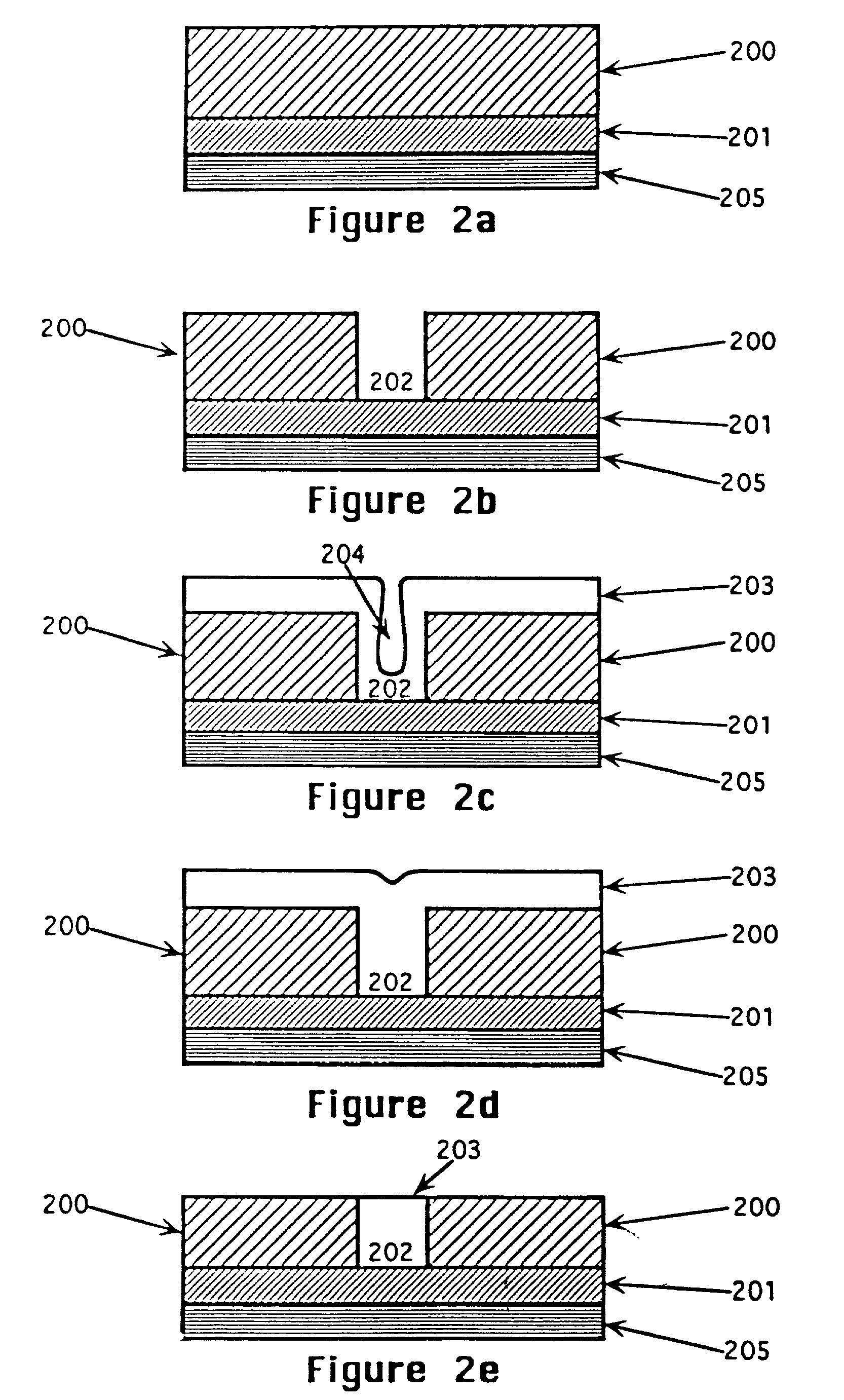
Figure 3
Abstract
Description
[0001] The present invention relates to semiconductor processing, and more particularly to a method of forming copper interconnections in a semiconductor device.
[0002] As the demand for cheaper, faster, lower power consuming microprocessors increases, so must the device packing density of the integrated circuit. Very large scale integration (VLSI) techniques have continually evolved to meet the increasing demand. All aspects of the integrated circuit must be scaled down to fully minimize the device dimensions of the integrated circuit. In addition to minimizing transistor dimensions, one must minimize the dimensions of the electrical interconnections which integrate the semiconductor devices, such as transistors, together on a microchip in order to form a complete circuit.
[0003] Currently, aluminum alloys are the most commonly used conductive materials for electrical interconnections in a VLSI integrated circuit. Aluminum and its alloys have been fully characterized for use as elect...
Examples
Embodiment Construction
[0031] A manufacturable method for forming a highly reliable, electrical interconnection is described which is particularly well suited for advanced VLSI and ULSI applications. In the following description, numerous specific details such as layer thicknesses, process sequences, times, temperatures, etc. are set forth in order to provide a more thorough understanding of the present invention. It will be obvious, however, to one skilled in the art, that the present invention may be practiced without employing these specific details. In other instances, well-known processes and processing techniques have not been described in detail in order not to unnecessarily obscure the present invention.
[0032] While diagrams representing a preferred embodiment of the present invention are illustrated in FIGS. 2a-3e, these illustrations are not intended to limit the invention. The specific processes described herein are only meant to help clarify an understanding of the present invention and to ill...