
Method for forming, by CVD, nanostructures of semi-conductor material of homogeneous and controlled size on dielectric material
a technology of semiconductor materials and nanostructures, which is applied in the direction of nanotechnology, crystal growth process, chemical vapor deposition coating, etc., can solve the problems of affecting the correct operation of the device, limiting the quality and performance of the device based on the structure, and high dispersion in size, around 50%, of silicon nanocrystals
Patent Information
- Authority / Receiving Office
- US · United States
- Patent Type
- Applications(United States)
- Current Assignee / Owner
- Publication Date
- 2004-07-29
Smart Images
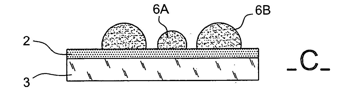
Figure 1 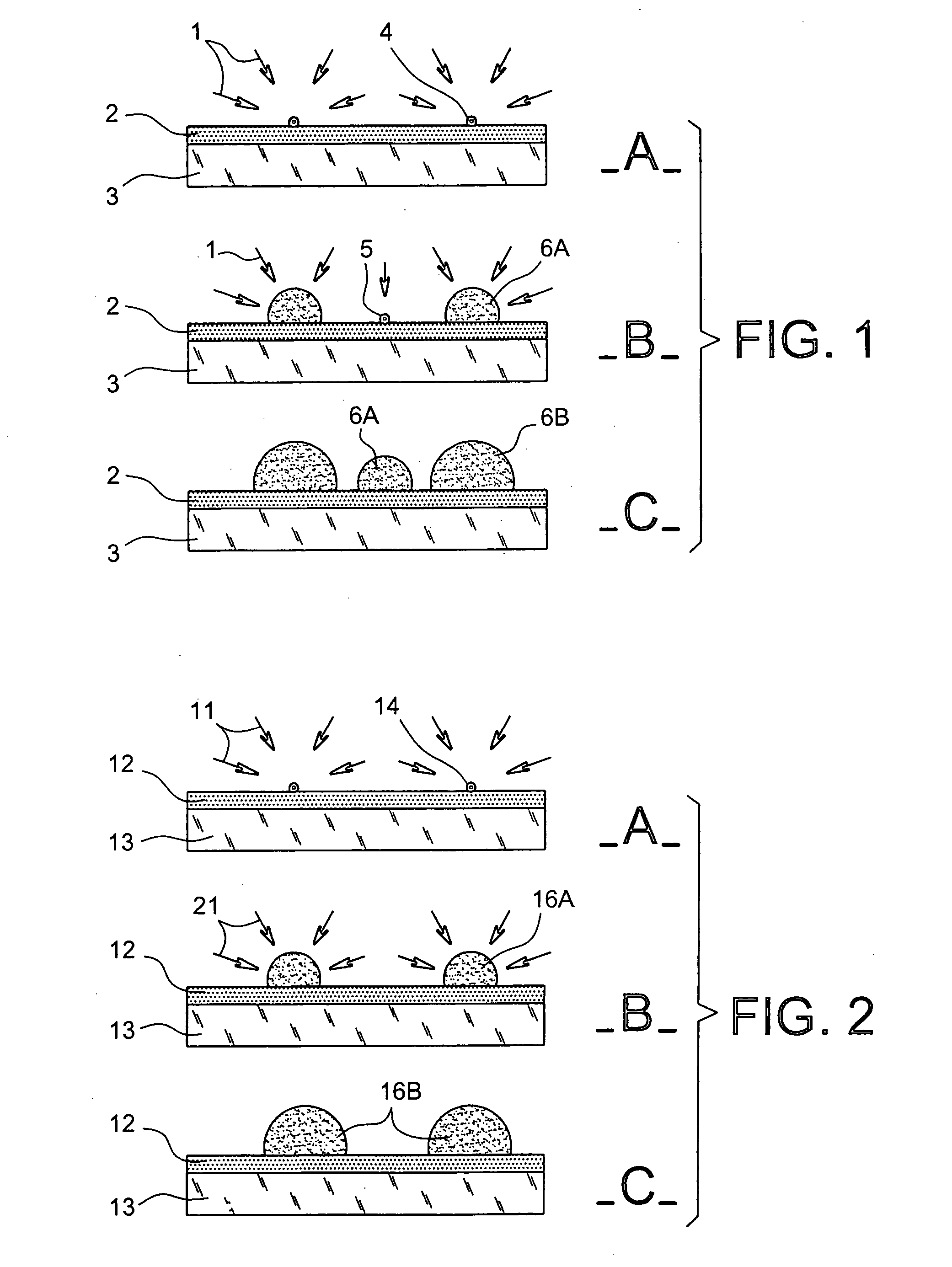
Figure 2
Abstract
Description
[0001] This application claims priority to French application no. 02 14658, filed on Nov. 22, 2002, entitled: "A Method For Forming, by CVD, Nanostructures of Semi-Conductor Material of Homogenous and Controlled Size on Dielectric Material" and was not published in English.
[0002] The invention concerns a method for forming nanostructures of semi-conductor material on a dielectric material by chemical vapour deposition (CVD), said nanostructures being of homogeneous and controlled size. The semi-conductor material is, in particular, silicon or germanium.
[0003] The invention further concerns devices with nanostructures obtained by means of the method according to the invention.
[0004] The nanostructures formed in this way are intended for forming electronic, optic or opto-electronic devices and, in particular, for forming Coulomb blockade devices that use quantum dots.
[0005] The applications targeted in particular by the present invention are granular gate storage cells and DOTFET, whi...
Examples
first embodiment
[0022] the first and second semi-conductor materials are in silicon.
second embodiment
[0023] the first semi-conductor material is in silicon and the second semi-conductor material is in germanium.
[0024] In other words, the method according to the invention makes it possible, firstly, to deposit nanostructures of germanium isolated from each other on a dielectric material by CVD; if the substrate of dielectric material is in silica and one uses germane as precursor of germanium, one does not need, thanks to said method, to deposit an intermediate continuous layer of silicon on the substrate of dielectric material of silica. By said method, the nanostructures have a homogeneous and controlled size, and their density varies between 10.sup.9 and some 10.sup.12 / cm.sup.2. Advantageously, by playing on the temperature and pressure parameters of the precursor during the deposition, one can obtain either crystalline or amorphous nanostructures.
[0025] Furthermore, the invention also makes it possible to deposit, on a dielectric material, nanostructures of silicon isolated fro...