
Electro-optical device, method of manufacturing the same, and electronic apparatus
Patent Information
- Authority / Receiving Office
- US · United States
- Current Assignee / Owner
- Publication Date
- 2005-03-03
Smart Images
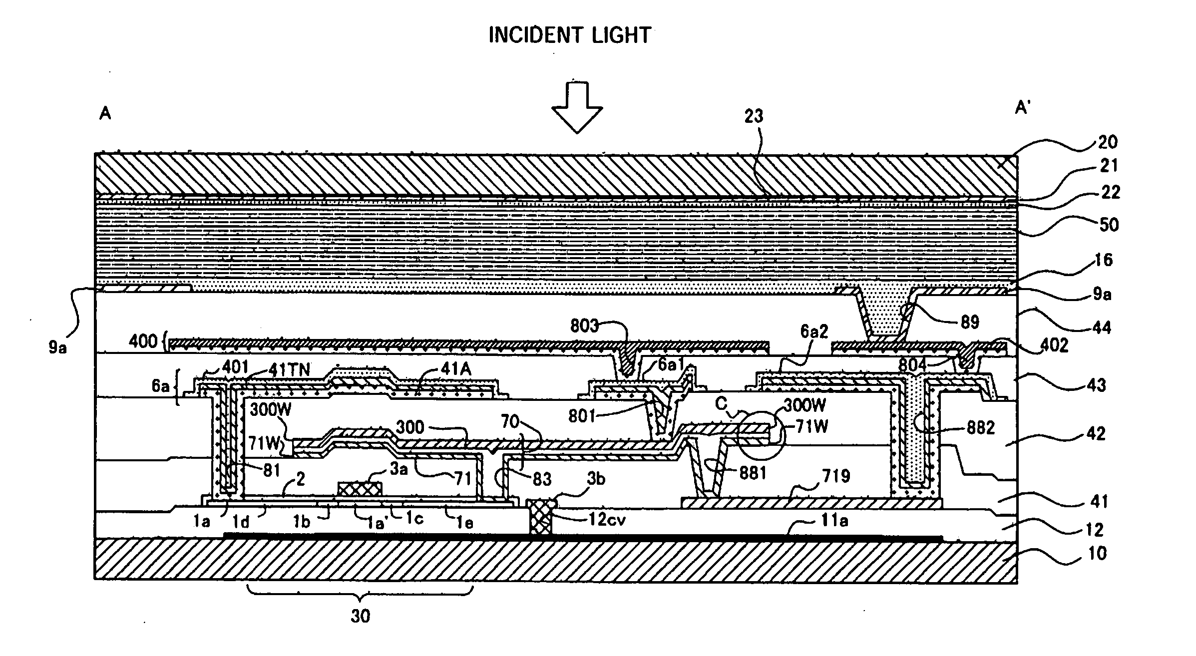
Figure 1 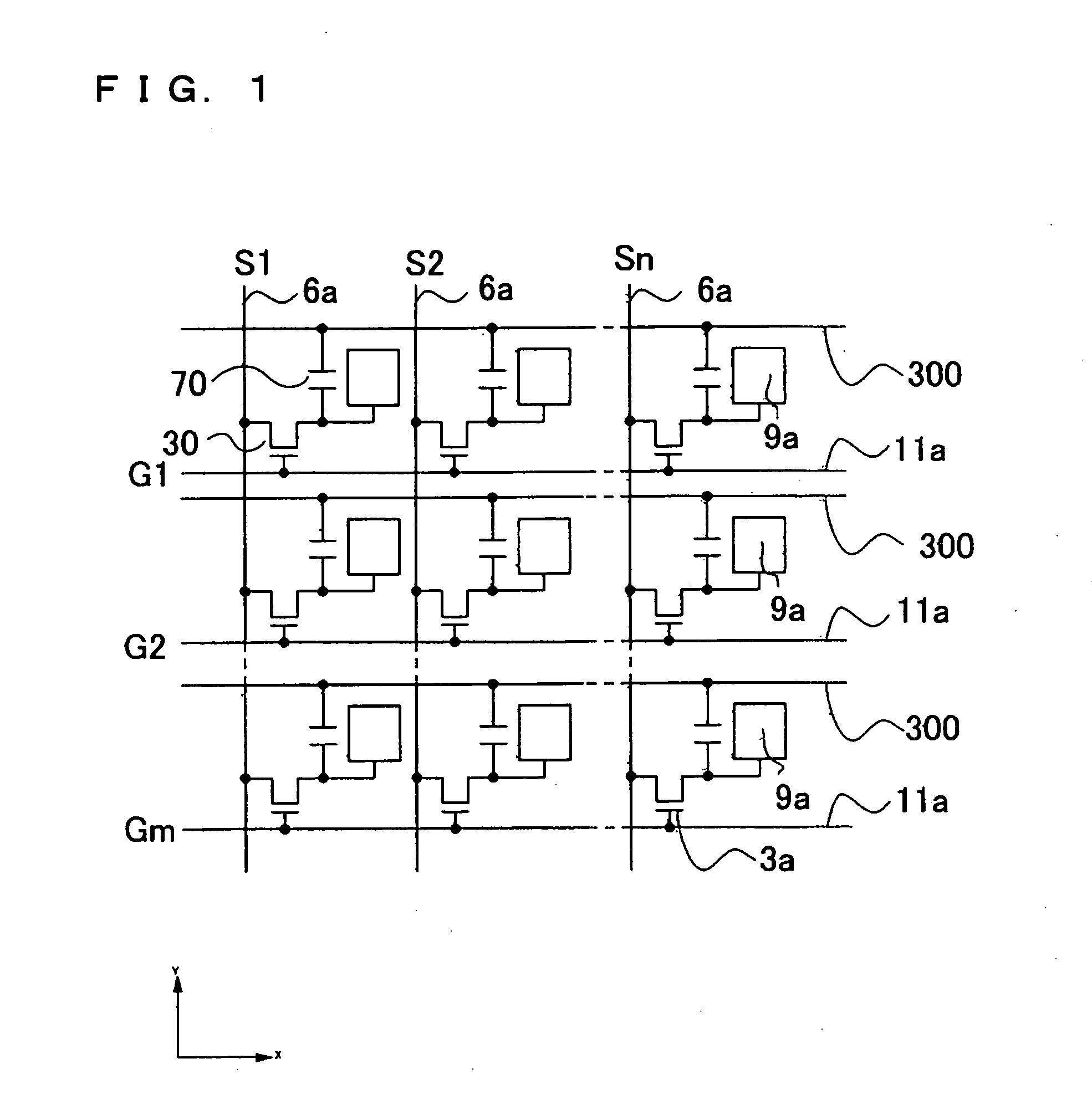
Figure 2 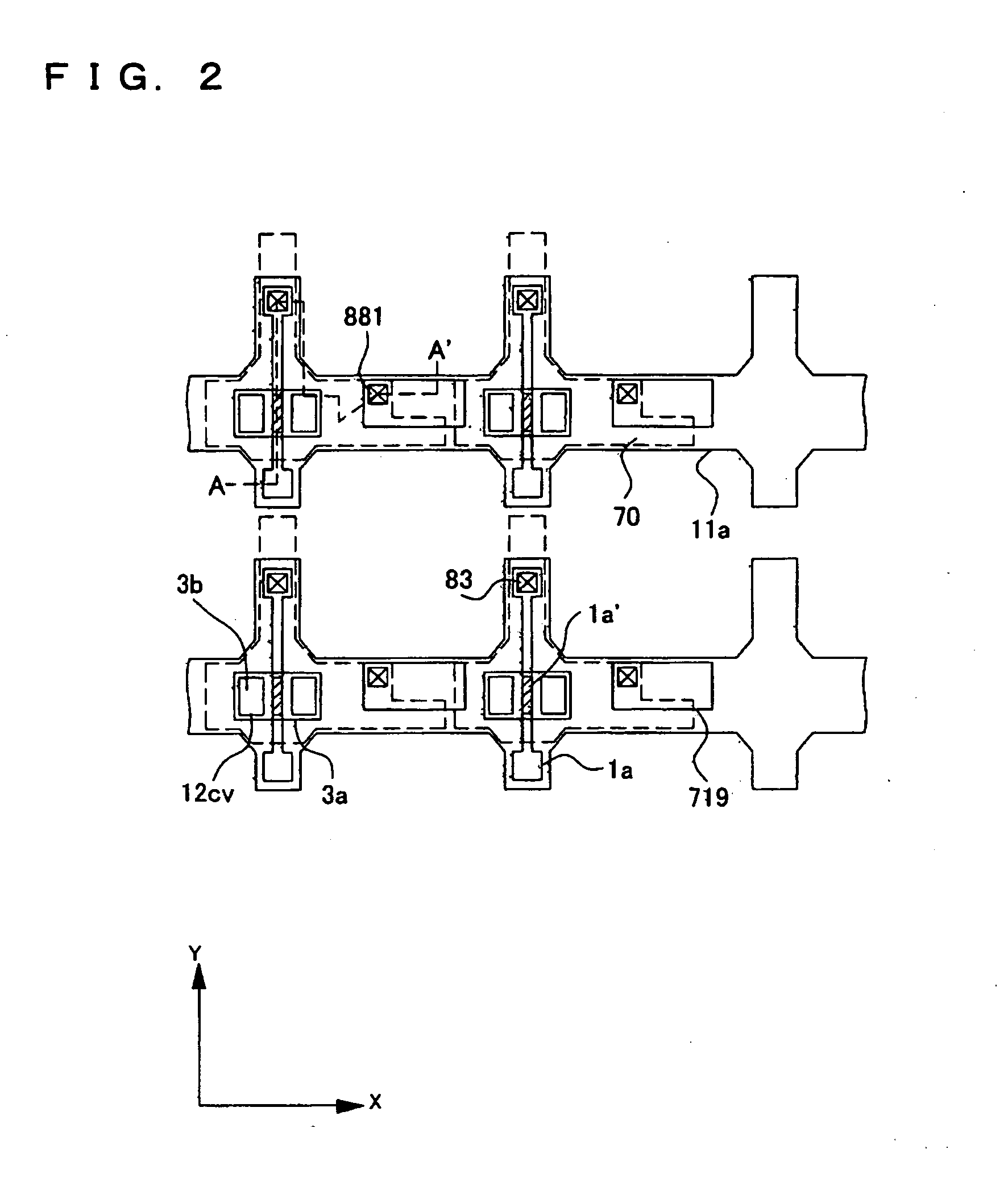
Figure 3
Abstract
Description
BACKGROUND OF THE INVENTION
[0001] 1. Field of Invention
[0002] The present invention relates to electro-optical devices such as an active-matrix-driving liquid crystal device, an electrophoresis device such as electronic paper, an electro-luminescent (EL) display device, and a device including an electron emission element such as a field emission display and a surface-conduction electron-emitter display, and to a method for manufacturing the same. Also, the present invention relates to electronic apparatus including the electro-optical device.
[0003] 2. Description of Related Art
[0004] The related art includes electro-optical devices capable of active-matrix-driving. The related art electro-optical devices include pixel electrodes arranged on a substrate in a matrix, thin film transistors (TFT) connected to each of the pixel electrodes, and data lines and scanning lines connected to the TFTs and provided in parallel in column and row directions.
[0005] The electro-optical device o...
Examples
Embodiment Construction
[0095] Exemplary embodiments of the present invention will now be described with reference to the drawings. According to the exemplary embodiment, an electro-optical device according to the present invention is applied to a liquid crystal device.
[0096] The structure of a pixel portion of an electro-optical device according to an exemplary embodiment of the present invention will now be described with reference to FIGS. 1 to 4. Here, FIG. 1 is a schematic that shows an equivalent circuit of various elements, wiring lines, etc. in a plurality of pixels formed in a matrix that constitutes an image display region of the electro-optical device. FIGS. 2 and 3 are schematics that show plan views of a plurality of pixel groups adjacent to each other on a TFT array substrate on which data lines, scanning lines, and pixel electrodes are formed. Also, FIGS. 2 and 3 respectively illustrate a lower portion (FIG. 2) and an upper portion (FIG. 3) in a laminated structure to be described later. FI...