
Surface emitting semiconductor laser, its manufacturing method, and manufacturing method of electron device
a manufacturing method and semiconductor technology, applied in semiconductor devices, lasers, semiconductors, etc., can solve the problems of difficult high-frequency driving, difficult high-frequency driving, and difficult control of lateral mode oscillation, etc., to reduce current constriction diameter, easy to manufacture, and high yield
Patent Information
- Authority / Receiving Office
- US · United States
- Patent Type
- Applications(United States)
- Current Assignee / Owner
- Publication Date
- 2005-12-08
- Estimated Expiration
- Not applicable · inactive patent
Smart Images
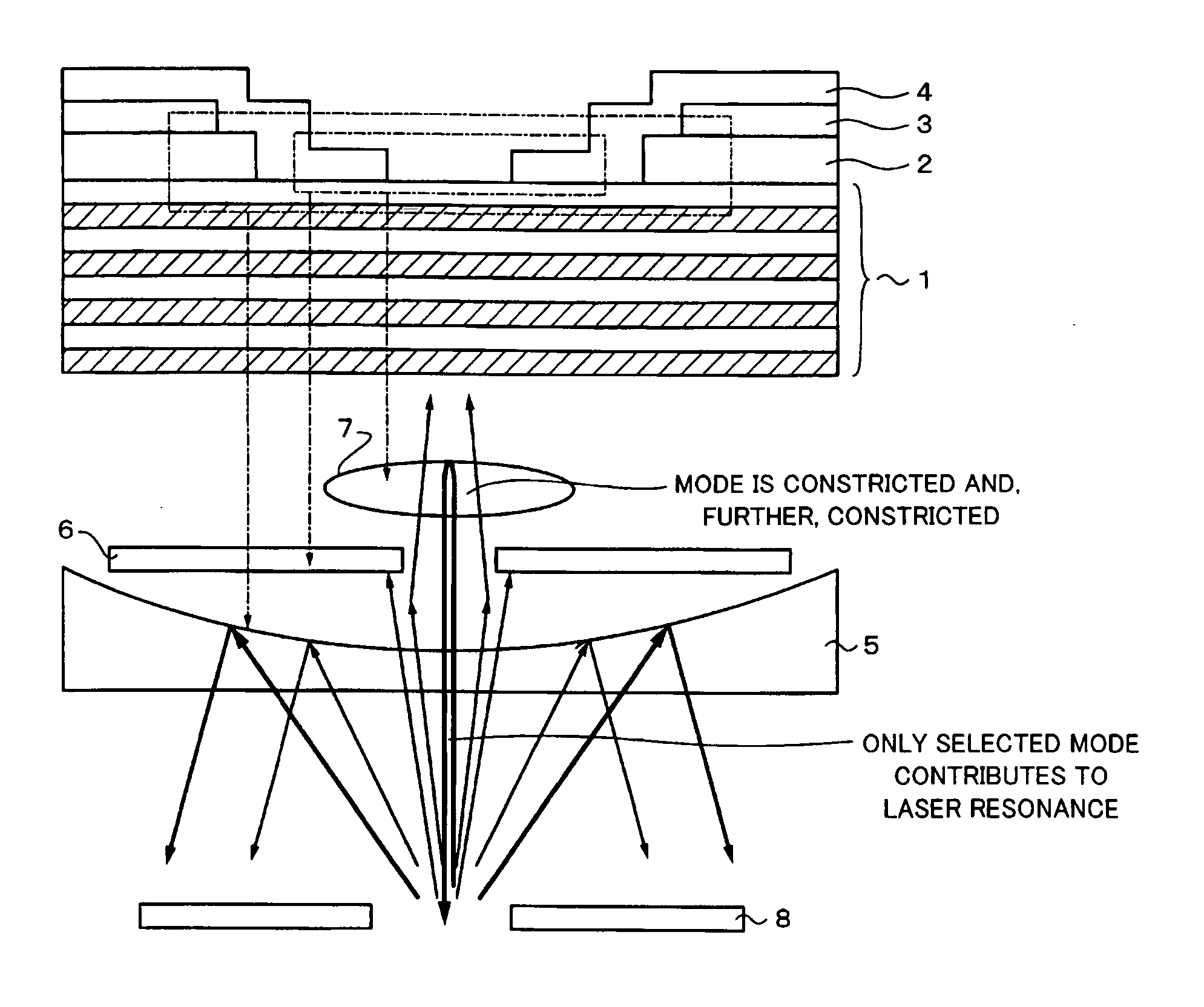
Figure 1 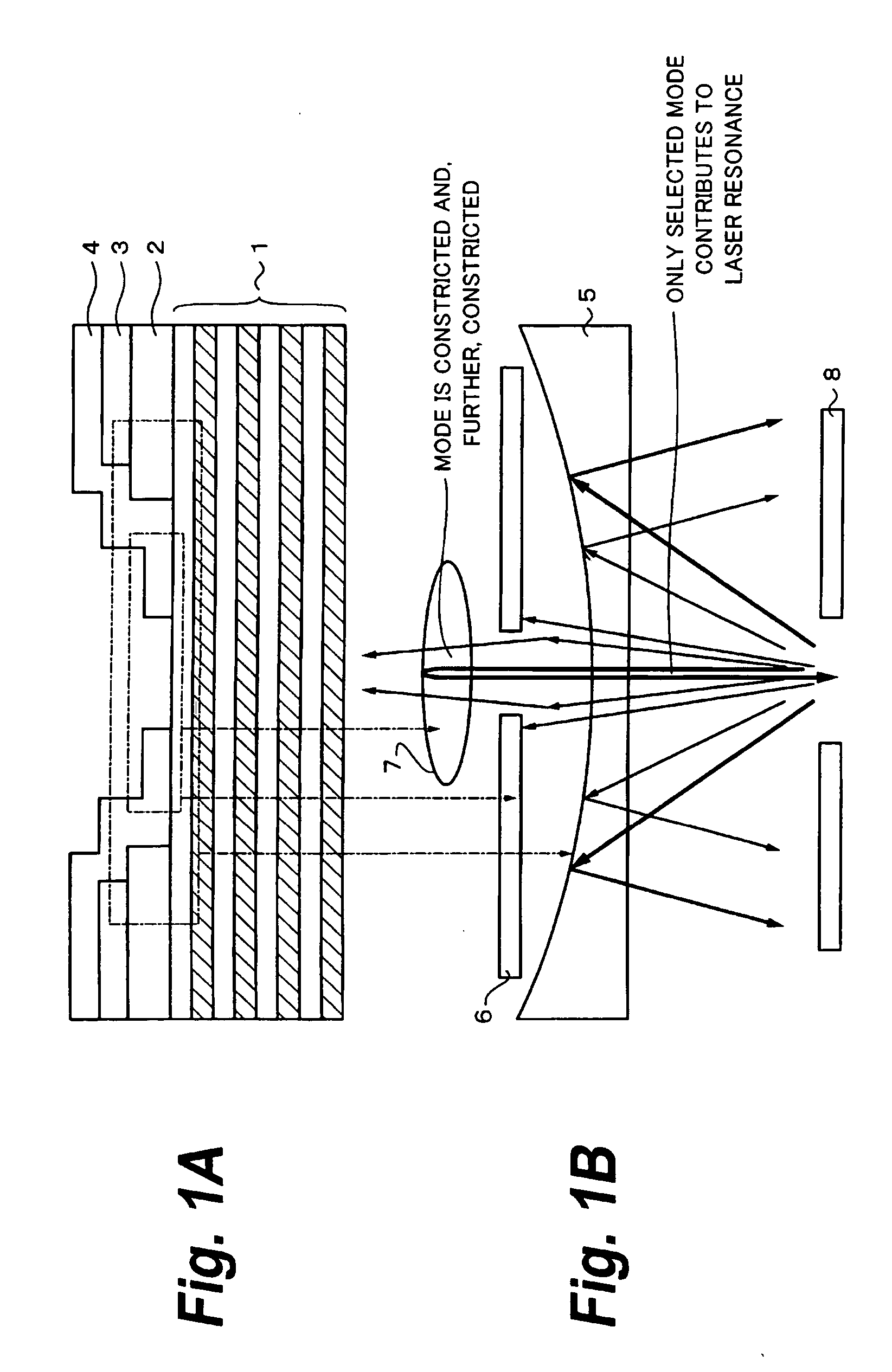
Figure 2 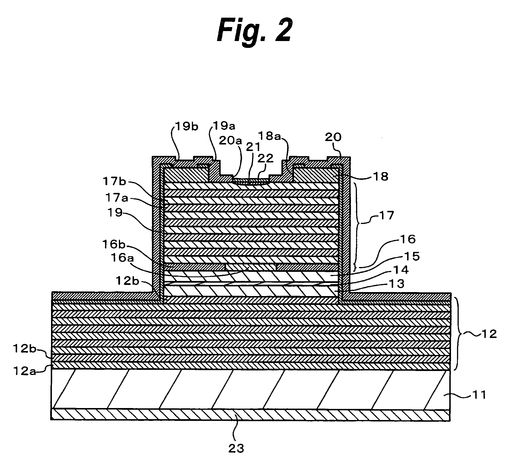
Figure 3
Abstract
Description
CROSS REFERENCES TO RELATED APPLICATIONS
[0001] The present invention contains subject matter related to Japanese Patent Application No. 2004-166869 filed in the Japanese Patent Office on Jun. 4, 2004, the entire contents of which being incorporated herein by reference. BACKGROUND OF THE INVENTION
[0002] 1. Field of the Invention
[0003] The invention relates to a surface emitting semiconductor laser, its manufacturing method, and a manufacturing method of an electron device.
[0004] 2. Description of the Related Arts
[0005] In recent years, attention has been paid to a VCSEL (Vertical Cavity Surface Emitting Laser) as a laser for optical communication. Such a surface emitting laser has a structure in which upper and lower surfaces of an active layer are sandwiched between an n-type reflective layer and a p-type reflective layer. Generally, a DBR (Distributed Bragg Reflector) made of a semiconductor multilayer film is used for each of the n-type reflective layer and the p-type reflect...
Examples
Embodiment Construction
[0054] Embodiments of the invention will be described hereinbelow with reference to the drawings. The same or corresponding portions in all of the drawings of the embodiments are designated by the same reference numerals.
[0055]FIG. 2 is a cross sectional view showing a surface emitting semiconductor laser according to the embodiment of the invention. FIG. 3 is a plan view of a mesa post portion of the surface emitting semiconductor laser. FIG. 4 is an enlarged cross sectional view of portions near a light outgoing portion of the surface emitting semiconductor laser.
[0056] As shown in FIGS. 2 to 4, in the surface emitting semiconductor laser, for example, an n-type DBR layer 12, a lower clad layer 13, an active layer 14 as a light-emitting layer, an upper clad layer 15, a current constriction layer 16, a p-type DBR layer 17, and a p-type contact layer 18 are sequentially laminated on an n-type semiconductor substrate 11 like an n-type GaAs substrate.
[0057] The n-type DBR layer 12 ...