
Low power content addressable memory system and method
Patent Information
- Authority / Receiving Office
- US · United States
- Current Assignee / Owner
- Publication Date
- 2006-08-03
- Estimated Expiration
- Not applicable · inactive patent
Smart Images
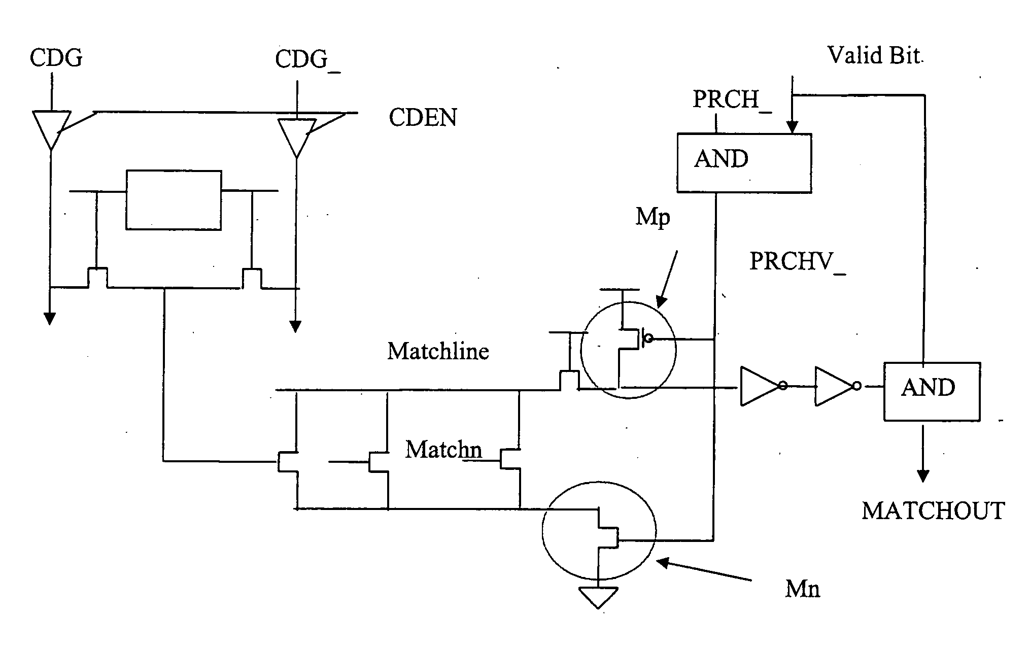
Figure 1 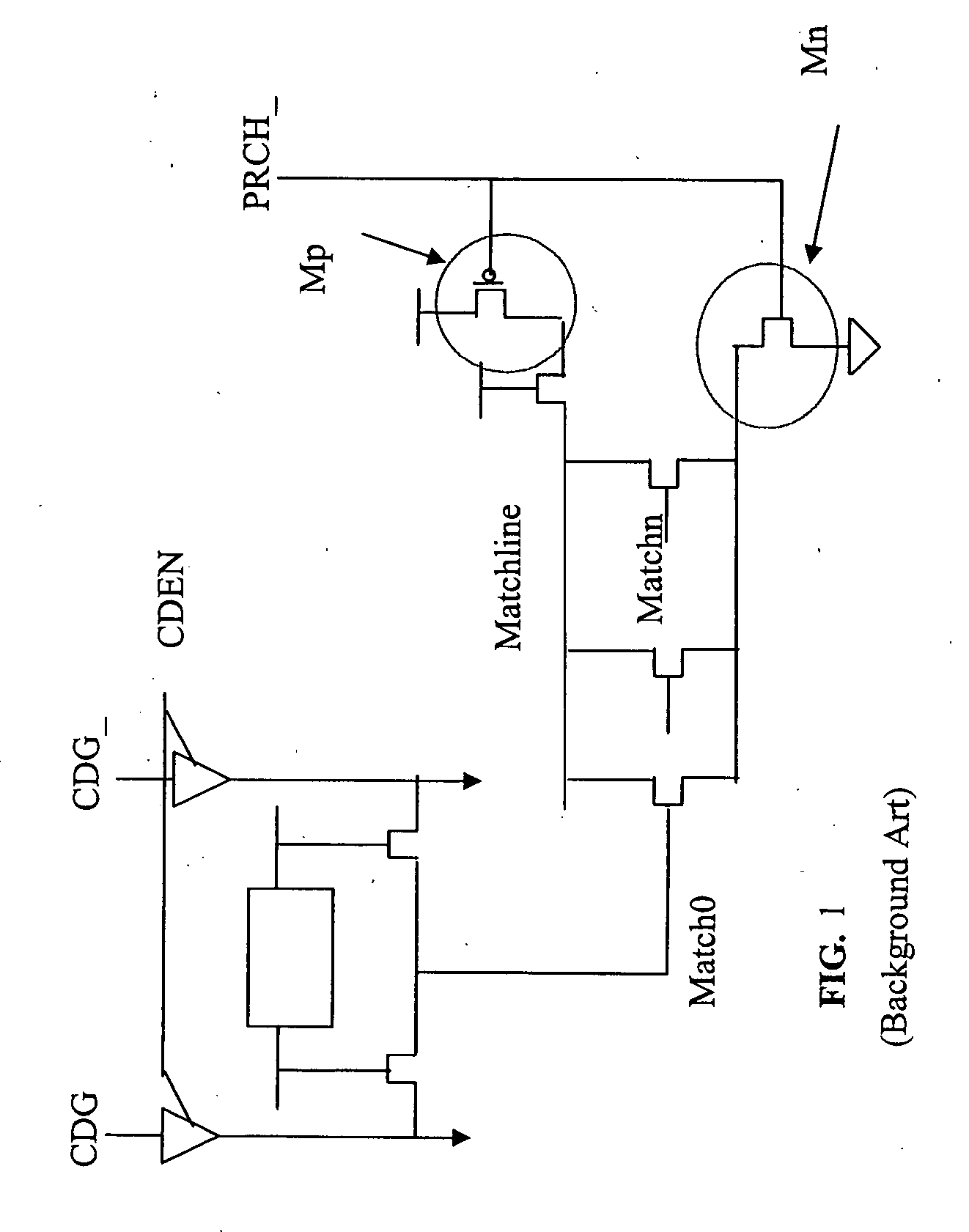
Figure 2 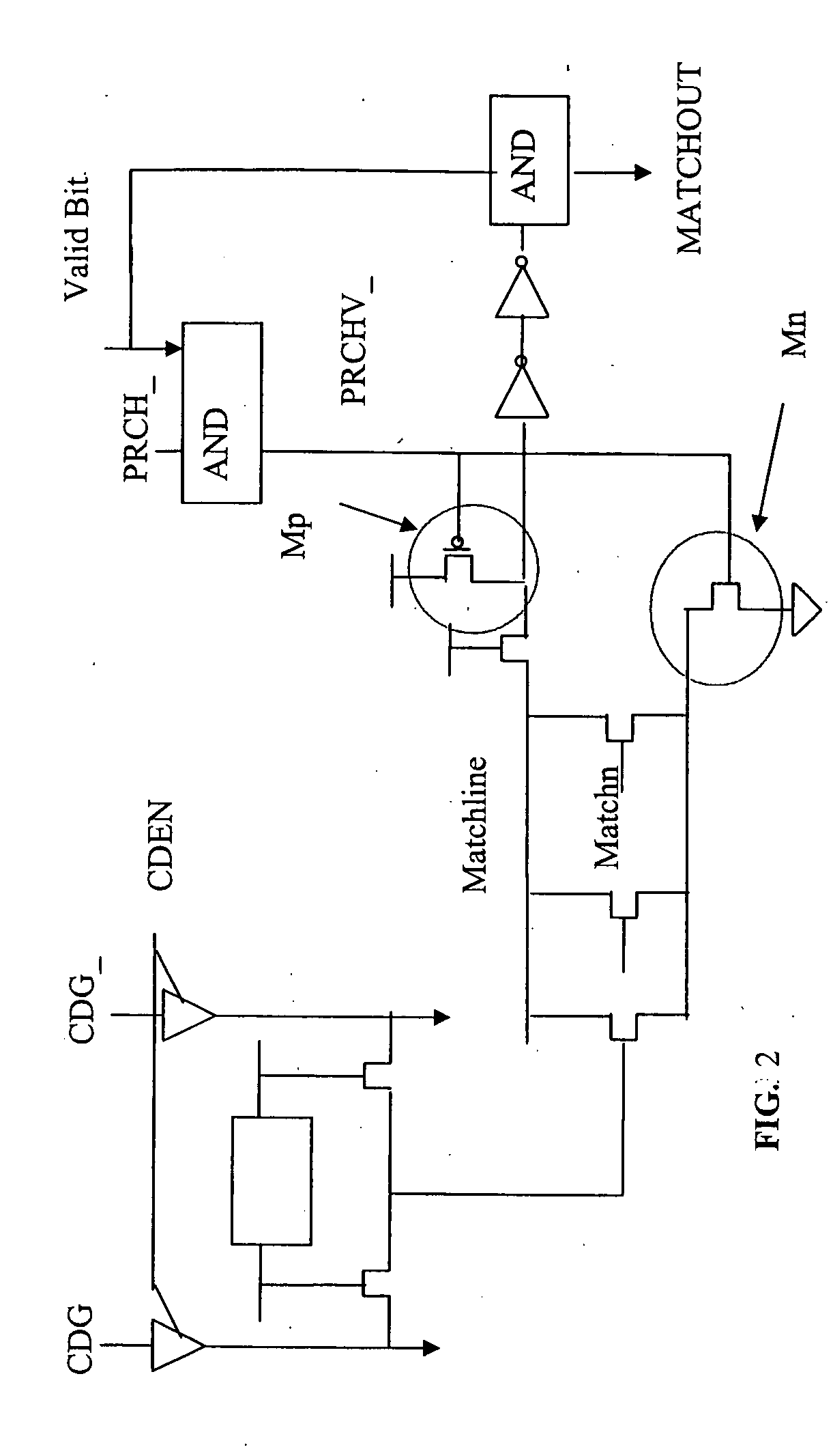
Figure 3
Abstract
Description
PRIORITY CLAIM
[0001] This application claims priority from Indian patent application No. 2593 / Del / 2004, filed Dec. 29, 2004, which is incorporated herein by reference. TECHNICAL FIELD
[0002] The present invention provides a low power content addressable memory system by restricting searches to valid entries. BACKGROUND
[0003] High densities CAMs (Content Addressable Memory) are most widely used for IP lookup / packet classifications operations in routers. The CAM circuits consume a good amount of power during lookup operations.
[0004] FIG. 1 shows the search operation for a conventional high density CAM. For example, if the size of memory is M words for each of N bits and number of match lines is M then all the M match lines are precharged to vdd-vt through a PRCH_signal. In the worst case, if there is no data match or a hit condition, all the match lines would discharge. If average discharge current through one match line is IMatch then the worst case discharge current is M×Imatch, w...
Examples
Embodiment Construction
[0014] The following discussion is presented to enable a person skilled in the art to make and use the invention. Various modifications to the embodiments will be readily apparent to those skilled in the art, and the generic principles herein may be applied to other embodiments and applications without departing from the spirit and scope of the present invention. Thus, the present invention is not intended to be limited to the embodiments shown, but is to be accorded the widest scope consistent with the principles and features disclosed herein.
[0015]FIG. 2 shows a CAM cell storing a tag bit with each word. If this bit is set, it indicates that the word is a valid entry else it is not a valid entry. The valid bit is logically ANDed with the PRCH_signal by using the logic and gate AND, to thereby enable the bit match operation and is then applied at the gates of the PMOS Mp and NMOS Mn. For a given word, if the valid bit is set then only match line evaluation of that particular word ...