
Method of correcting mask pattern and correcting apparatus thereof
a mask pattern and mask technology, applied in the field of photolithographic apparatus and operating method thereof, can solve the problems of inability to accurately transfer the pattern, serious impact on the accuracy of the pattern and the process window, and the susceptibility of the pattern on the mask to the corner rounding effect, so as to achieve high accuracy and increase the reliability and throughput of production. , the effect of high accuracy
Patent Information
- Authority / Receiving Office
- US · United States
- Current Assignee / Owner
- Publication Date
- 2007-01-25
Smart Images
Figure 1 
Figure 2 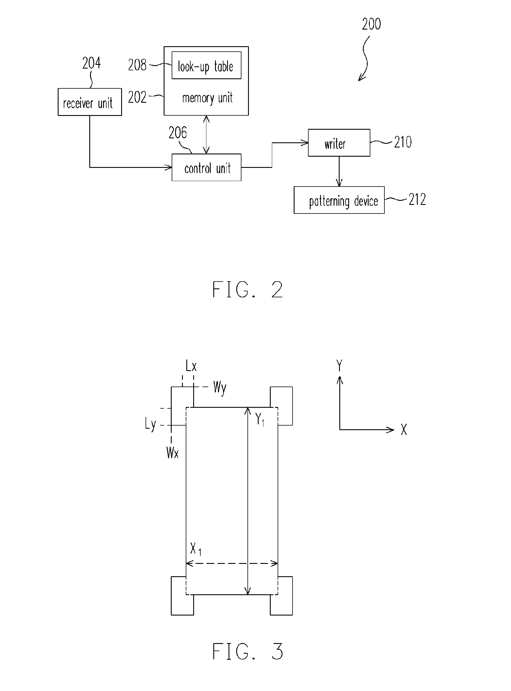
Figure 3
Abstract
Description
BACKGROUND OF THE INVENTION
[0001] 1. Field of the Invention
[0002] The present invention relates to a photolithographic apparatus and operating method thereof, and more particularly, to a method of correcting mask pattern and correcting apparatus thereof.
[0003] 2. Description of the Related Art
[0004] In recent years, the trend in the development of semiconductor is miniaturization of circuit devices. Among the processes used in semiconductor production, photolithographic process plays a very important role. Critical dimensions (CD) concerning semiconductor device structures, such as patterning various thin films, are dependent on the photolithographic process, which also determine the development of photolithographic technology. Thus, the accuracy of a photomask pattern is very crucial. If the pattern on the photomask is inaccurate, an inaccurate pattern will be transferred. Hence, the tolerance of the critical dimension on the chip can be affected and the resolution of the expos...
Examples
Embodiment Construction
[0026] Reference will now be made in detail to the present preferred embodiments of the invention, examples of which are illustrated in the accompanying drawings. Wherever possible, the same reference numbers are used in the drawings and the description to refer to the same or like parts.
[0027] Due to dimensional deviation problem, and particularly, corner rounding problem, most mask patterning methods have undesirable consequences in subsequent fabricating processes such as a drop in the reliability and throughput and an increase in the production cost. Therefore, in the following embodiment, a mask pattern correcting apparatus and a correcting method thereof is provided.
[0028]FIG. 2 is a block diagram showing a mask pattern correcting apparatus according to one embodiment of the present invention.
[0029] As shown in FIG. 2, the mask pattern correcting apparatus 200 of the present invention comprises a memory unit 202, a receiver unit 204 and a control unit 206. The memory unit 2...