
Substrate-guided optical devices
a technology of optical devices and substrates, applied in the field of substrate-guided optical devices, can solve the problems of high cost where high-performance is required, inconvenient installation, unsafe use, etc., and achieve the effect of convenient incorporation and convenient structure and fabrication of compact devices
Patent Information
- Authority / Receiving Office
- US · United States
- Patent Type
- Applications(United States)
- Current Assignee / Owner
- Publication Date
- 2007-04-26
Smart Images
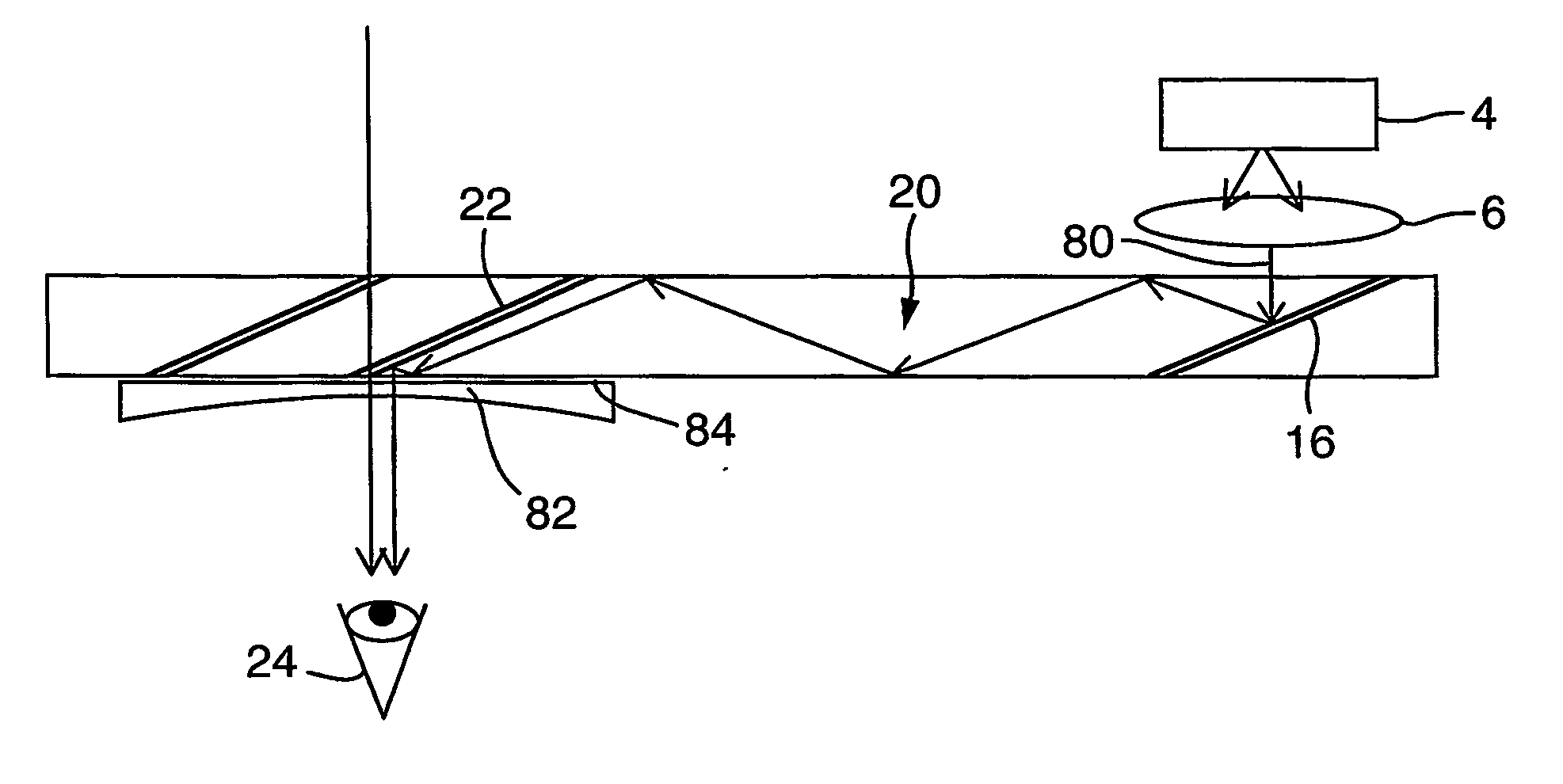
Figure 1 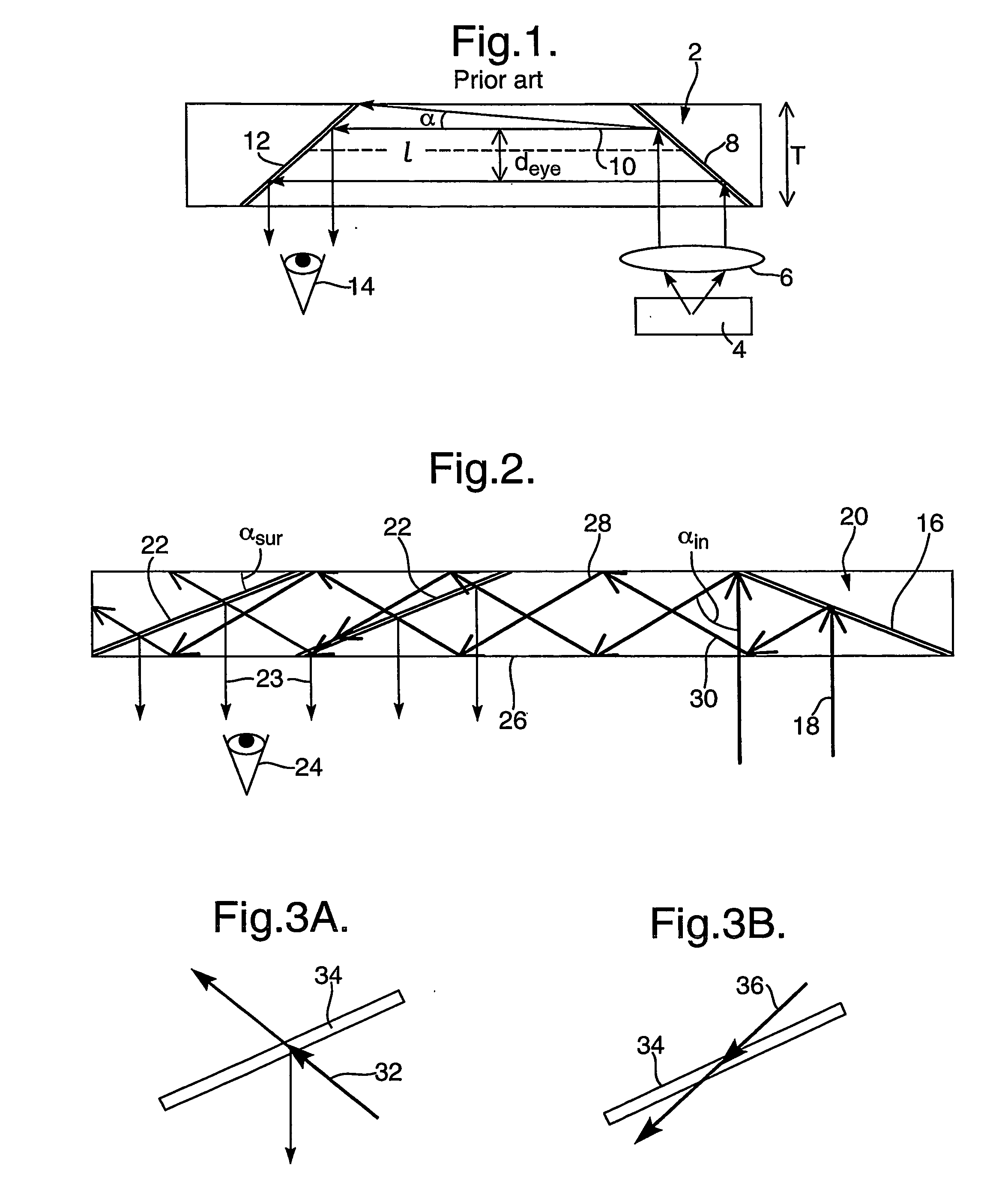
Figure 2 
Figure 3
Abstract
Description
[0001] The present invention relates to substrate-guided optical devices, and particularly to devices which include a plurality of reflecting surfaces carried by a common light-transmissive substrate, also referred to as a light-guide.
[0002] The invention can be implemented to advantage in a large number of imaging applications, such as, for example, head-mounted and head-up displays (HMD's and HUD's), cellular phones, compact displays, 3-D displays, compact beam expanders, as well as non-imaging applications such as flat-panel indicators, compact illuminators and scanners. BACKGROUND OF THE INVENTION
[0003] One of the important applications for compact optical elements is in HMD's wherein an optical module serves both as an imaging lens and a combiner, in which a two-dimensional display is imaged to infinity and reflected into the eye of an observer. The display can be obtained directly from either a spatial light modulator (SLM) such as a cathode ray tube (CRT), a liquid crystal ...
Examples
Embodiment Construction
[0030]FIG. 1 illustrates a conventional folding optics arrangement, wherein the substrate 2 is illuminated by a display source 4. The display is collimated by a collimating lens 6. The light from the display source 4 is coupled into substrate 2 by a first reflecting surface 8, in such a way that the main ray 10 is parallel to the substrate plane. A second reflecting surface 12 couples the light out of the substrate and into the eye of a viewer 14. Despite the compactness of this configuration, it suffers significant drawbacks; in particular only a very limited FOV can be affected. As shown in FIG. 1, the maximum allowed off-axis angle inside the substrate is: αmax=arctan(T-deye2l),(1)
wherein T is the substrate thickness;
[0031] deye is the desired exit-pupil diameter, and
[0032] l is the distance between reflecting surfaces 8 and 12.
[0033] With angles higher than αmax the rays are reflected from the substrate surface before arriving at the reflecting surface 12. Hence, the refl...