
Circuit design system and circuit design program
a circuit design and circuit technology, applied in the field of circuit design system and circuit design system program, can solve the problems of low occurrence rate and unnecessarily inserting observation points, and achieve the effect of fewer observation points, efficient facilitation of failure analysis, and improved failure analysis
Patent Information
- Authority / Receiving Office
- US · United States
- Patent Type
- Applications(United States)
- Current Assignee / Owner
- Publication Date
- 2007-05-17
Smart Images
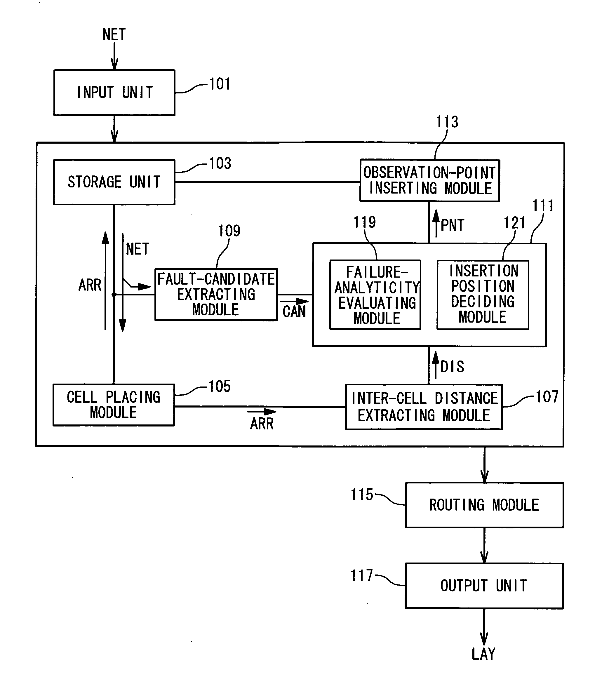
Figure 1 
Figure 2 
Figure 3
Abstract
Description
BACKGROUND OF THE INVENTION
[0001] 1. Field of the Invention
[0002] The present invention relates to a circuit design system and a circuit design system program used in designing a logic circuit. In particular, the present invention relates to a circuit design system and a circuit design system program used for facilitating a failure analysis.
[0003] 2. Description of the Related Art
[0004] In an ordinary process of manufacturing semiconductor integrated circuits, defective products are included in the manufactured semiconductor integrated circuits to some degree. The defective products are eliminated in a test process and only non-defective products are shipped. Here, a rate of the non-defective products at this time is referred to as “yield”. If the yield is low, then cost of manufacturing goods is increased and profit is declined. It is therefore necessary to establish a cause of the defect by a failure analysis and to enhance the yield by improving the manufacturing process. [00...
Examples
first embodiment
1. First Embodiment
[0052]FIG. 3 is a block diagram showing a configuration of a circuit design system (a failure analysis facilitating design system) according to a first embodiment of the present invention. The circuit design system shown in FIG. 3 generates a layout data LAY indicating a layout of a design-target circuit from a netlist NET indicating connection information of the design-target circuit. The circuit design system can be realized by, for example, a processing unit, a storage unit, and a computer program (circuit design program) executed by the processing unit.
[0053] Firstly, a general description will be given on the circuit design system according to the present embodiment. As shown in FIG. 3, the circuit design system has an input unit 101, a storage unit 103, a cell placing module 105, an inter-cell distance extracting module 107, a fault-candidate extracting module 109, a judgment module 111, an observation-point inserting module 113, a routing module 115, and a...
second embodiment
2. Second Embodiment
[0112]FIG. 14 is a block diagram showing a configuration of a circuit design system (a failure analysis facilitating design system) according to a second embodiment of the present invention. The circuit design system according to the present embodiment has the input unit 101, the storage unit 103, the cell placing module 105, the fault-candidate extracting module 109, the judgment module 111, the observation-point inserting module 113, the routing module 115, and the output unit 117. In FIG. 14, the same reference numerals are given to the same components as those described in the first embodiment, and an overlapping description will be appropriately omitted.
[0113] The second embodiment differs from the first embodiment in that the circuit design system does not include the inter-cell distance extracting module 107. Furthermore, in the second embodiment, the cell placing module 105 places cells after all the necessary observation points are inserted.
[0114]FIG. ...
third embodiment
3. Third Embodiment
[0122]FIG. 16 is a block diagram showing a configuration of a circuit design system (a failure analysis facilitating design system) according to a third embodiment of the present invention. The circuit design system according to the present embodiment has the input unit 101, the storage unit 103, the fault-candidate extracting module 109, a layout module 135, a judgment module 111, the observation-point inserting module 113, and the output unit 117. The layout module 135 includes the cell placing module 105 and the routing module 115. The judgment module 111 includes not only the failure-analyticity evaluating module 119 and the insertion position deciding module 121 but also a structure extracting module 123. In FIG. 16, the same reference numerals are given to the same components as those described in the first embodiment, and an overlapping description will be appropriately omitted.
[0123] The third embodiment differs from the first embodiment in that the circu...