
Method for manufacturing material layer, method for manufacturing ferroelectric capacitor using the same, ferroelectric capacitor manufactured by the same method, semiconductor memory device having ferroelectric capacitor and manufacturing method thereof
a manufacturing method and material layer technology, applied in the direction of capacitors, semiconductor devices, electrical equipment, etc., can solve the problems of affecting the operation reliability of the resulting semiconductor memory device, etc., to achieve the effect of improving the operation reliability and sufficient capacitan
Patent Information
- Authority / Receiving Office
- US · United States
- Patent Type
- Applications(United States)
- Current Assignee / Owner
- Publication Date
- 2008-09-04
- Estimated Expiration
- Not applicable · inactive patent
Smart Images
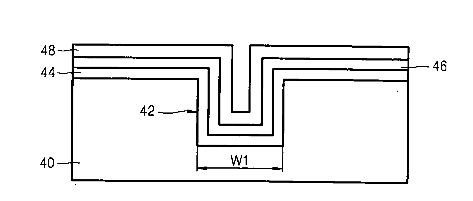
Figure 1 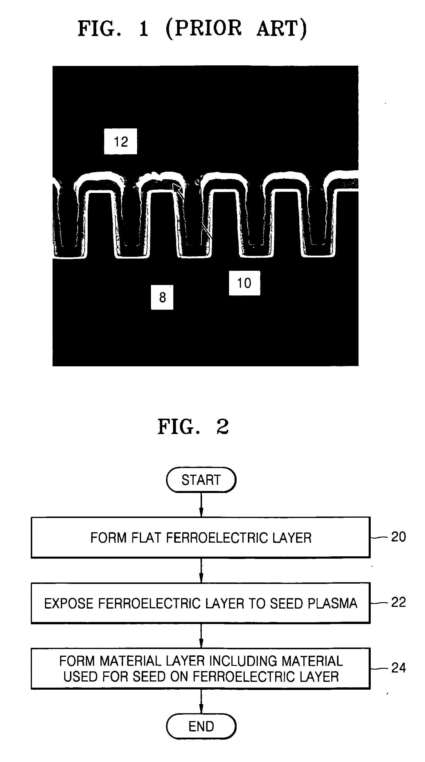
Figure 2 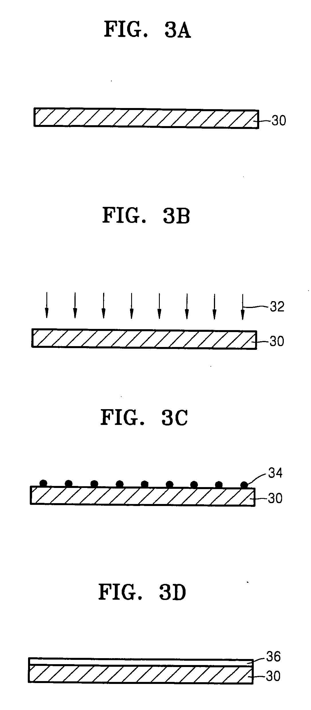
Figure 3
Abstract
Description
PRIORITY STATEMENT
[0001] This application claims the benefit of Korean Patent Application No. 10-2005-0063302, filed on Jul. 13, 2005, in the Korean Intellectual Property Office, the disclosure of which is incorporated herein in its entirety by reference.BACKGROUND
[0002] 1. Field
[0003] Example embodiments relate to a method for depositing a material layer, for example, a method for manufacturing a material layer capable of increasing the deposition rate of a noble metal layer on a ferroelectric layer, a method for manufacturing a ferroelectric capacitor using the same, a ferroelectric capacitor manufactured by the same method, and a semiconductor memory device having the ferroelectric capacitor and a manufacturing method thereof.
[0004] 2. Description of the Related Art
[0005] Semiconductor devices may be roughly classified into random access memories (RAMs) having volatility and which are freely read and written, and read only memories (ROMs) having non-volatility and which are read only....
Examples
Embodiment Construction
[0042]Example embodiments will now be described more fully with reference to the accompanying drawings. In the drawings, the thicknesses of layers and regions are exaggerated for clarity. Example embodiments will now be described more fully hereinafter with reference to the accompanying drawings. This invention may, however, be embodied in many different forms and should not be construed as being limited to the example embodiments set forth herein. Rather, these example embodiments are provided so that this disclosure will be thorough and complete, and convey the scope of example embodiments to those skilled in the art. Like numbers refer to like elements throughout the specification.
[0043]It will be understood that when an element or layer is referred to as being “on”, “connected to” or “coupled to” another element or layer, it can be directly on, connected or coupled to the other element or layer or intervening elements or layers may be present. In contrast, when an element is ref...