
Film capacitor
a film capacitor and capacitor technology, applied in the field of film capacitors, can solve the problems of insufficient disclosure structure, failure of ceramic capacitors to have both self-healing function and self-protective function, etc., and achieve the effect of high withstand voltag
Patent Information
- Authority / Receiving Office
- US · United States
- Current Assignee / Owner
- Publication Date
- 2009-07-23
Smart Images
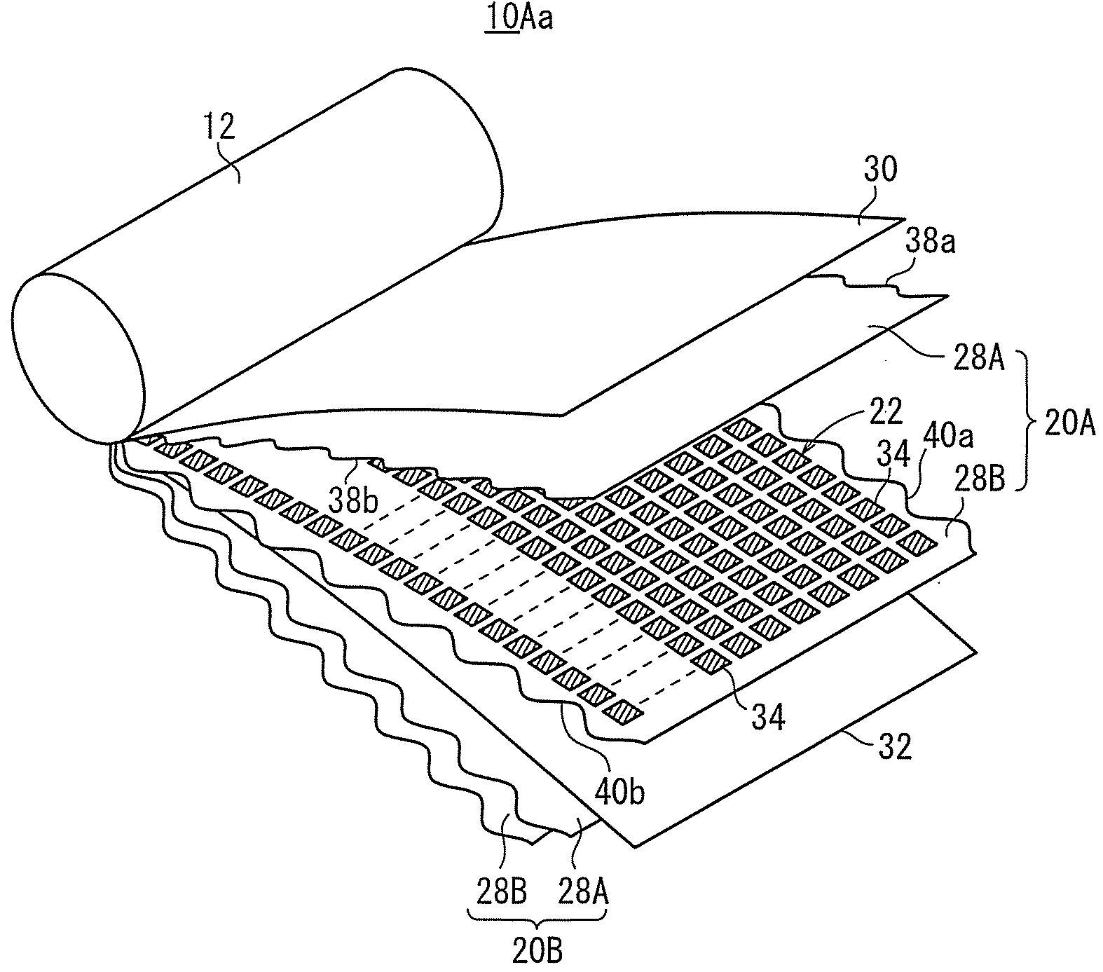
Figure 1 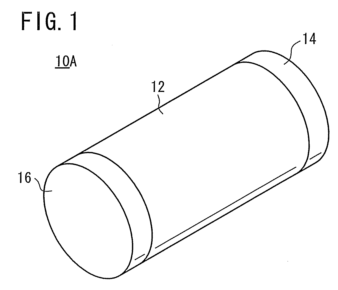
Figure 2 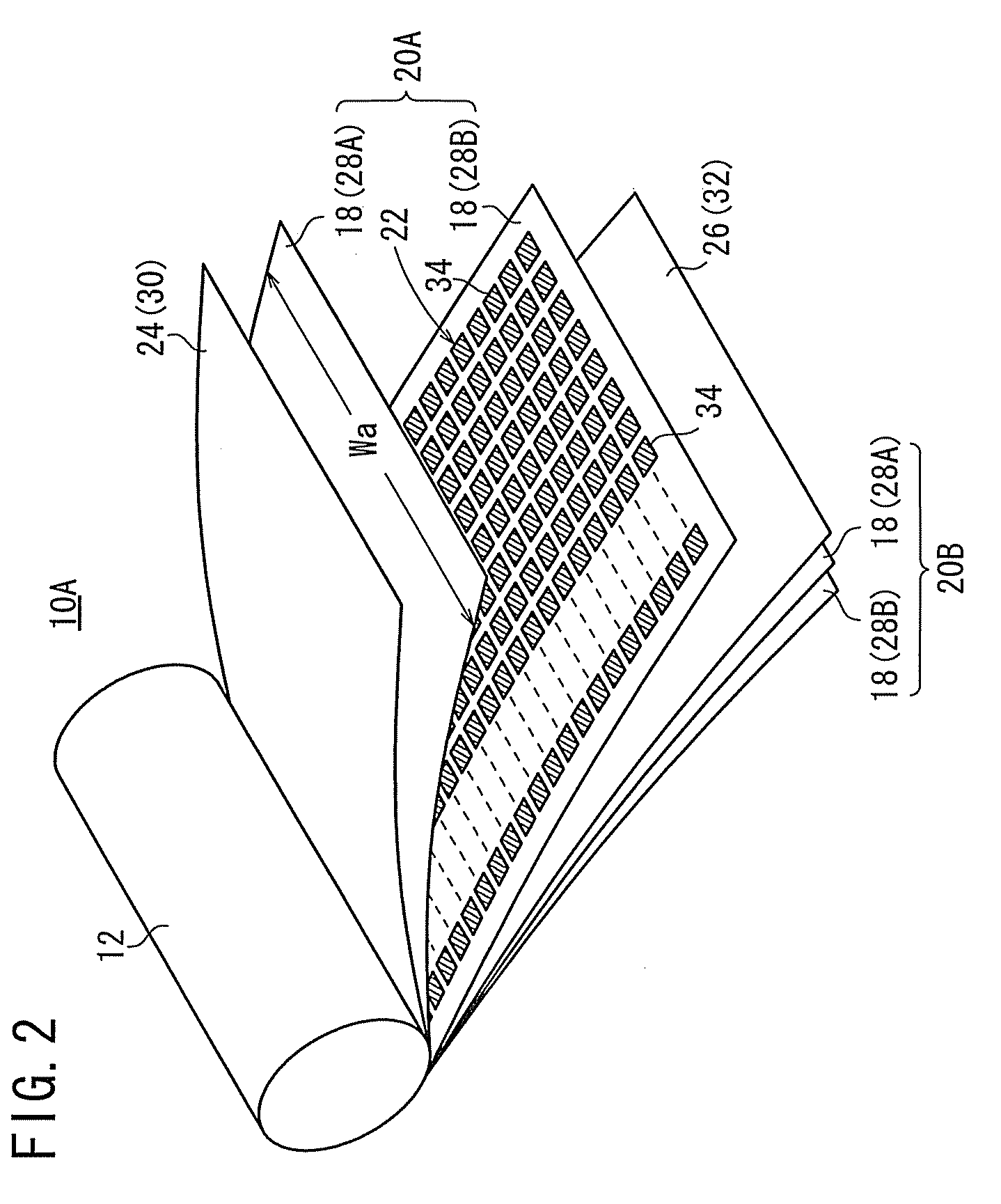
Figure 3
Abstract
Description
TECHNICAL FIELD
[0001] The present invention relates to a film capacitor comprising a rolled assembly of stacked films, which has a stack of dielectric films and includes a floating electrode therein, a first terminal electrically connected to one end of the roll, and a second terminal electrically connected to the other end of the roll, and more particularly to a film capacitor, which has a self-healing function and a self-protective function.BACKGROUND ART
[0002] Film capacitors having a self-healing function are disclosed in Patent Documents 1 through 4, for example.
[0003] The film capacitor disclosed in Patent Document 1 includes a pair of capacitor electrodes, which confront each other with a dielectric film sandwiched therebetween. At least one of the capacitor electrodes is formed by metal evaporation, and is divided equally into spaced or arbitrarily spaced intervals in the longitudinal direction of the film by a plurality of insulating grooves, thereby providing a plurality of s...
Examples
first embodiment
[0044]As shown in FIG. 1, a film capacitor according to the present invention (hereinafter referred to as a “first film capacitor 10A”) comprises a roll 12, a first terminal 14 electrically connected to an end of the roll 12, and a second terminal 16 electrically connected to another end of the roll 12.
[0045]As shown in FIG. 2, the roll 12 includes at least two stacked film assemblies (a first stacked film assembly 20A and a second stacked film assembly 20B) each comprising a stack of dielectric films 18.
[0046]The first stacked film assembly 20A and the second stacked film assembly 20B each includes a floating electrode 22 therein. The first stacked film assembly 20A is sandwiched between a first metal film 24 and a second metal film 26 disposed on opposite surfaces thereof.
[0047]The roll 12 comprises a coiled stack made up of the first metal film 24, the first stacked film assembly 20A, the second metal film 26, and the second stacked film assembly 20B.
[0048]As shown in FIGS. 2 and...
second embodiment
[0061]As shown in FIG. 7, a film capacitor according to the present invention (hereinafter referred to as a “second film capacitor 10B”) is of essentially the same structure as the first film capacitor 10A, but differs therefrom as follows.
[0062]Each of the first stacked film assembly 20A and the second stacked film assembly 20B comprises a stack of alternate first dielectric films 28A and second dielectric films 28B. In FIG. 7, the first stacked film assembly 20A comprises two stacks 50 made up of first dielectric films 28A and second dielectric films 28B. Similarly, the second stacked film assembly 20B comprises two stacks 50 made up of first dielectric films 28A and second dielectric films 28B.
[0063]The first metal foil 30 is disposed on the upper surface of the first dielectric film 28A that is positioned on an upper portion of the first stacked film assembly 20A, and the second metal foil 32 is disposed on the lower surface of the second dielectric film 28B that is positioned o...
third embodiment
[0068]As shown in FIG. 8, a film capacitor according to the present invention (hereinafter referred to as a “third film capacitor 10C”) is of essentially the same structure as the second film capacitor 10B, but differs therefrom as follows.
[0069]Each of the first stacked film assembly 20A and the second stacked film assembly 20B comprises four stacks 50 made up of first dielectric films 28A and second dielectric films 28B.
[0070]In the first stacked film assembly 20A, each of the small electrodes 34 of the floating electrode 22 on one of the second dielectric films 28B of the first stack (the stack 50 made up of the first dielectric film 28A and the second dielectric film 28B closest to the first metal foil 30) and the first metal foil 30 form a thirty-first capacitor C31 therebetween, and each of the small electrodes 34 of the floating electrode 22 on the second dielectric film 28B together with a corresponding one of the small electrodes 34 on the second dielectric film 28B of the ...