

Optical device manufacturing method
a manufacturing method and optical device technology, applied in the direction of manufacturing tools, after-treatment details, semiconductor lasers, etc., can solve the problems of poor productivity, difficult to simultaneously cut high-brittle optical device wafers and heat sink materials made of metal such as high-ductile copper, and achieve the effect of efficient manufacturing
Patent Information
- Authority / Receiving Office
- US · United States
- Patent Type
- Applications(United States)
- Current Assignee / Owner
- Publication Date
- 2009-09-17
Smart Images
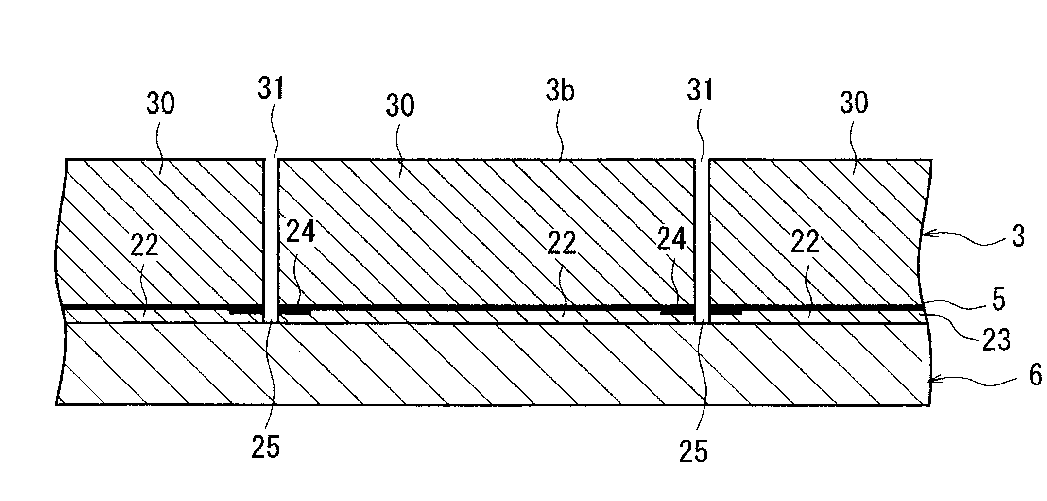
Figure 1 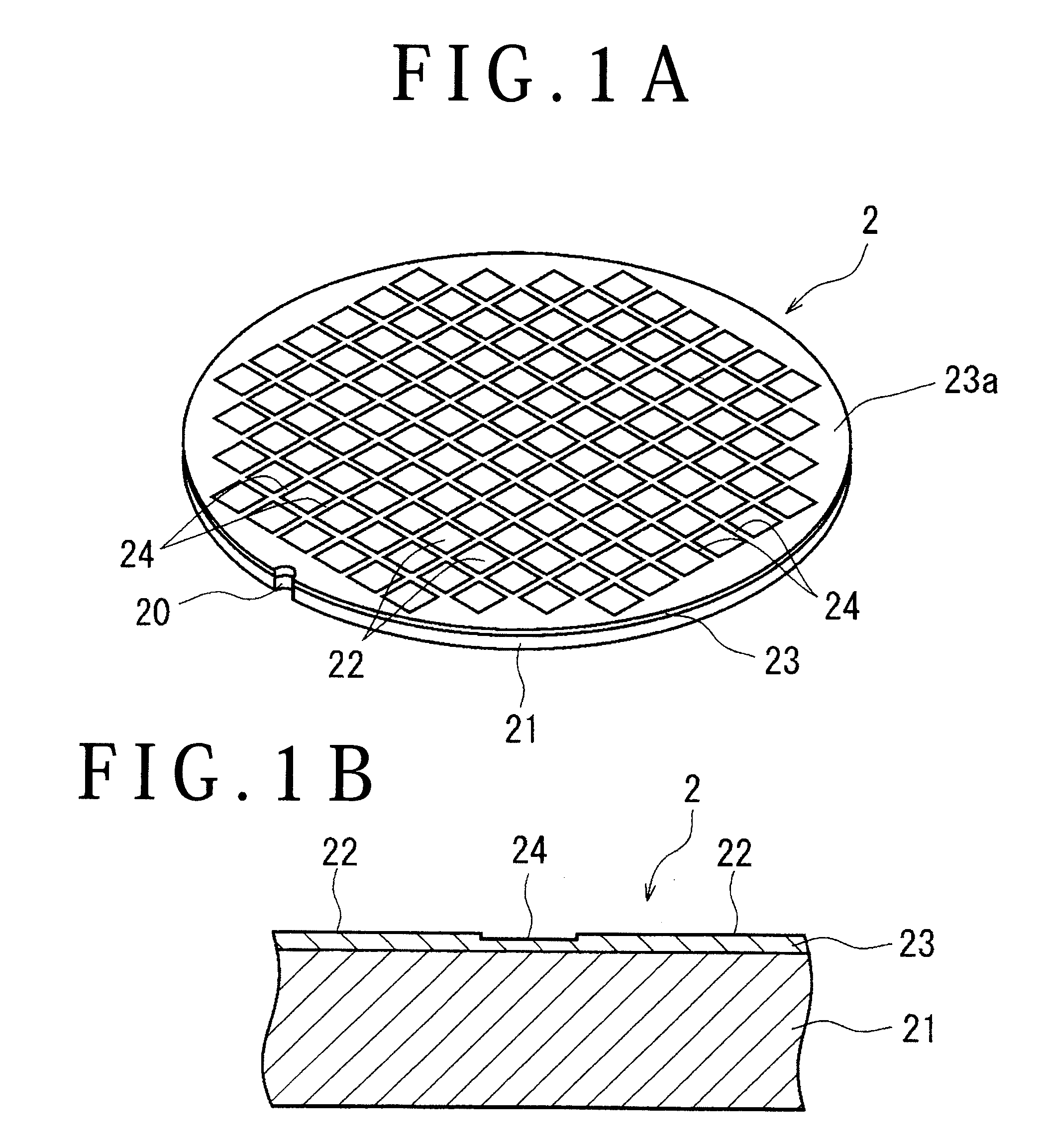
Figure 2 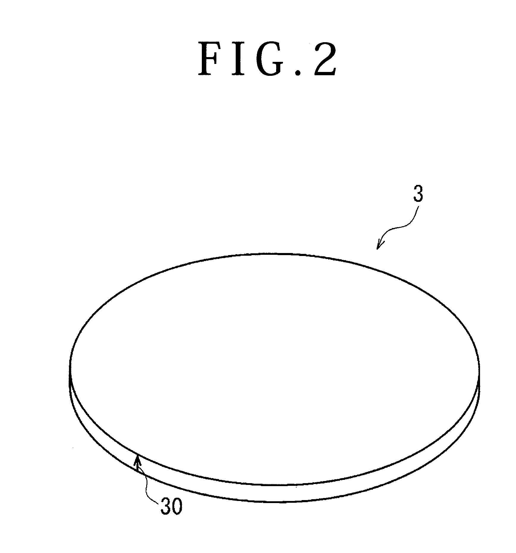
Figure 3
Abstract
Description
BACKGROUND OF THE INVENTION
[0001] 1. Field of the Invention
[0002] The present invention relates to an optical device manufacturing method of dividing an optical device wafer into a plurality of optical devices sectioned along streets and joining a heat sink to each of the optical devices, the optical device wafer being formed with the optical devices in an optical device layer lying on the front surface of a substrate.
[0003] 2. Description of the Related Art
[0004] In the optical device manufacturing step, a plurality of optical devices are formed in an optical device layer made of a gallium nitride-based compound semiconductor or the like on the front surface of a sapphire substrate, a silicon carbide substrate or the like. An optical device wafer formed with the optical devices in the optical device layer as mentioned above is divided into the individual optical devices sectioned along streets for manufacture.
[0005] As a method of dividing an optical device wafer along streets, a method...
Examples
Embodiment Construction
[0028]Preferred embodiments of an optical device manufacturing method according to the present invention will hereinafter be described in detail with reference to the accompanying drawings. An optical device wafer 2 illustrated in FIGS. 1A and 1B is such that an optical device layer 23 forming a plurality of optical devices 22 made of gallium nitride (GaN) or the like is formed on the front surface of a substrate 21 made of sapphire. Lattice-like streets 24 are formed on the front surface 23a of the optical device layer 23 so as to section the optical devices 22. The optical device wafer 2 is formed at an outer circumferential portion with a notch 20 indicating the crystal orientation of the sapphire substrate 21.
[0029]A description is below given of a first embodiment of the optical device manufacturing method in which the optical device wafer 2 is divided into the plurality of optical devices 22 sectioned along the streets 24 and a heat sink is joined to each of the optical device...