
Organic el device and electronic apparatus
Patent Information
- Authority / Receiving Office
- US · United States
- Current Assignee / Owner
- Publication Date
- 2010-04-08
Smart Images
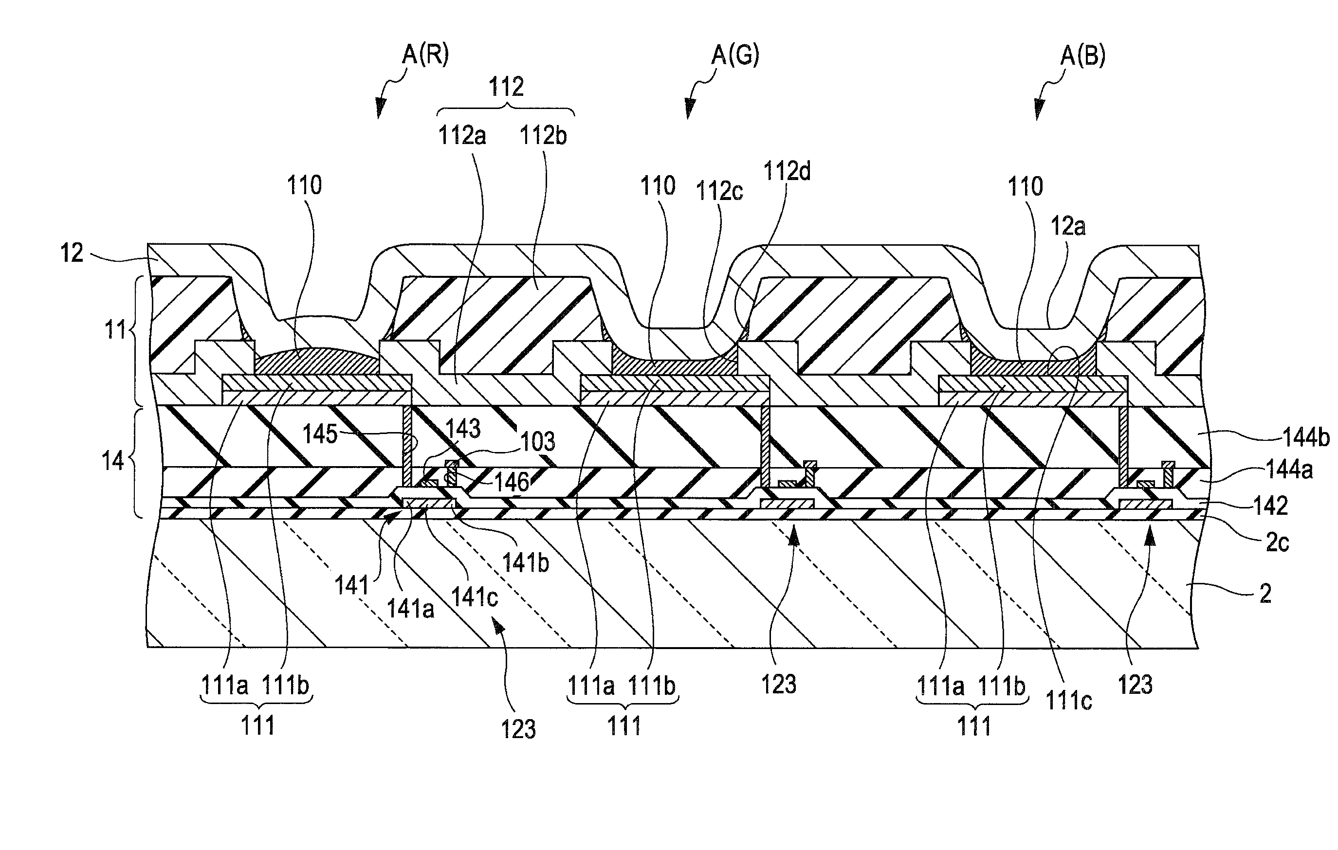
Figure 1 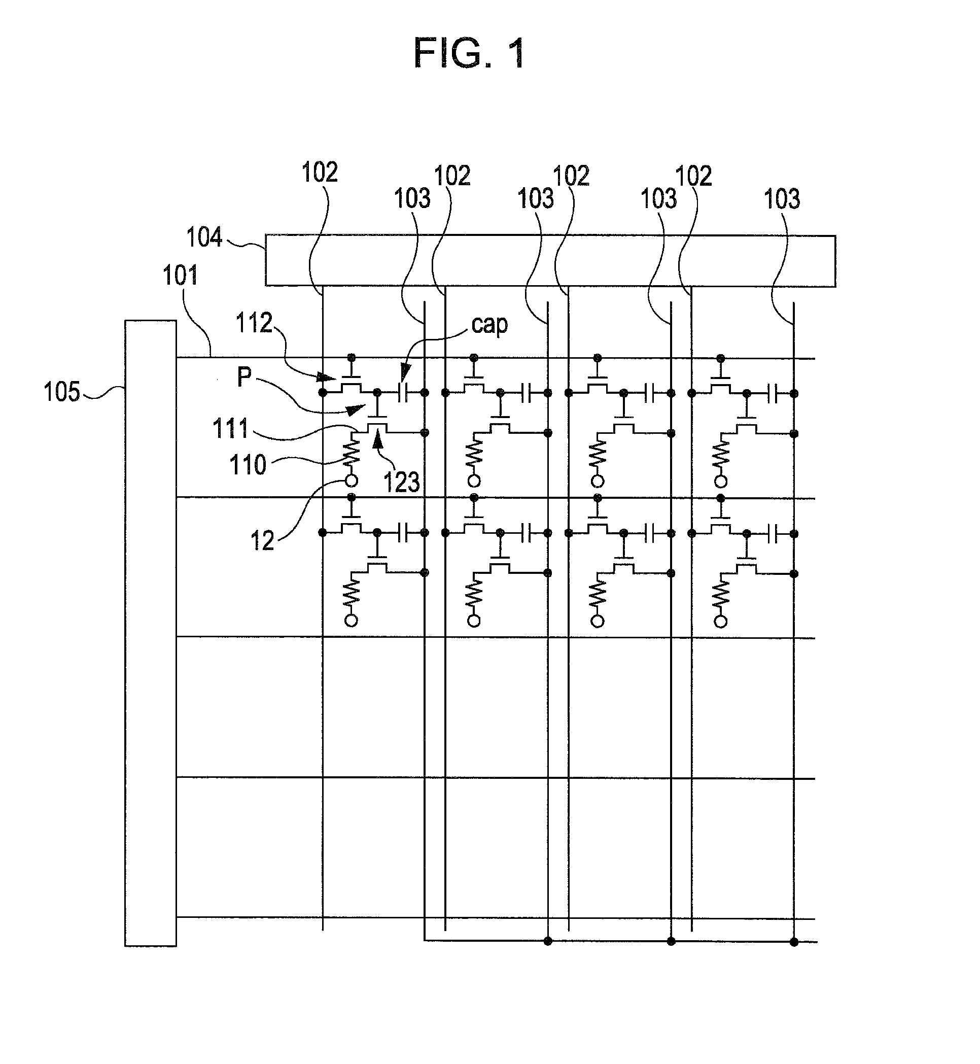
Figure 2 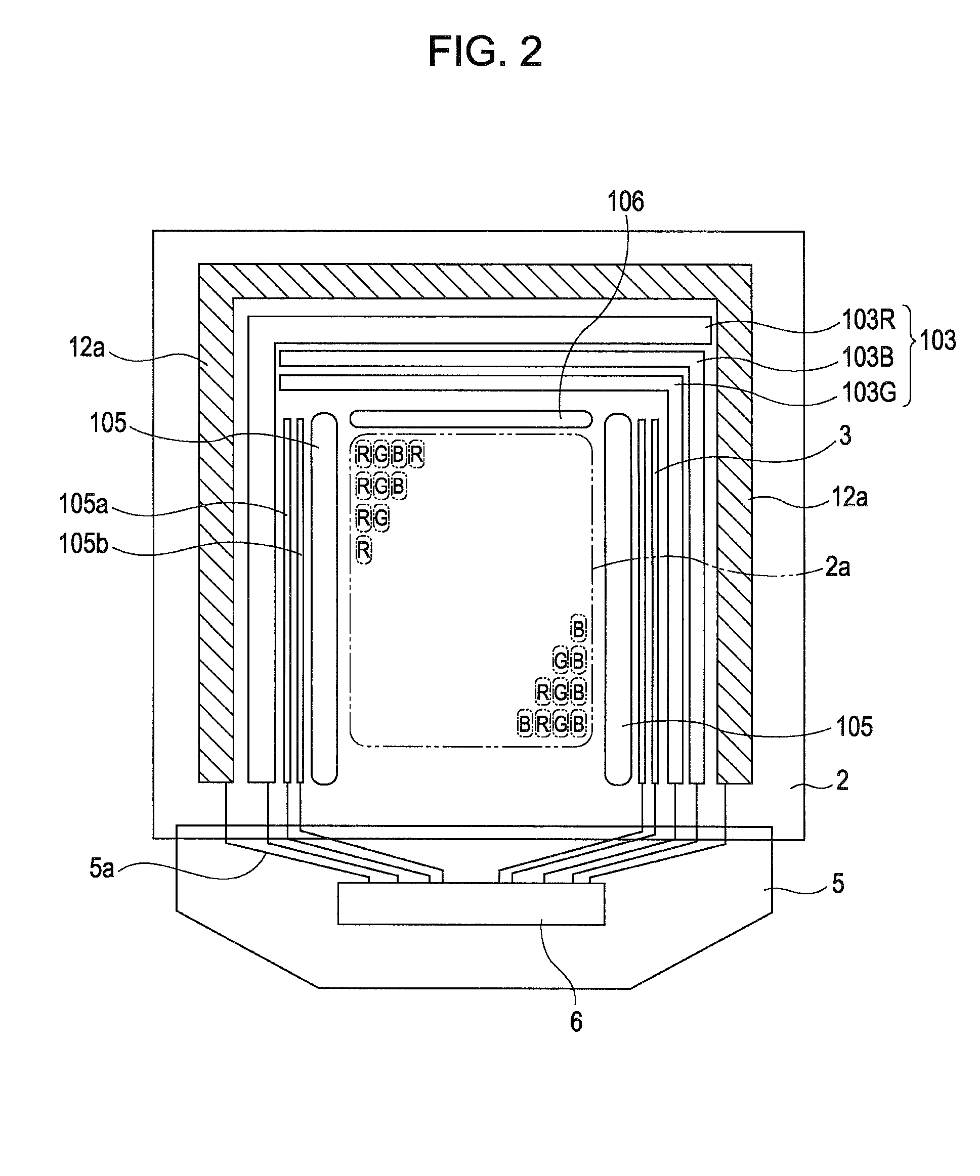
Figure 3
Abstract
Description
BACKGROUND
[0001] 1. Technical Field
[0002] The present invention relates to an organic EL device and an electronic apparatus.
[0003] 2. Related Art
[0004] Recently, as technology for forming a functional film such as a light emitting layer (functional layer) of an organic electroluminescence device (organic EL device) or a color filter film of a color liquid crystal device, technology in which the functional film is formed by coating a liquid-phase material including a functional film forming material by using a liquid droplet ejecting method such as an ink jet method and by drying the liquid-phase material has been known.
[0005] However, such a functional film has different functional characteristics depending on the thickness thereof. Accordingly, for example, among pixels of an organic EL device that implement emission of a red color (R), a green color, and a blue color (B), in order for the functional layers such as light emitting layers to exhibit the same function (characteristics) amo...
Examples
experimental examples
[0112]The relationship between the film thickness of the light emitting layer and the current efficiency of the light emitting element (organic EL element) was checked in the following manner.
[0113]As the light emitting element (organic EL element), the anode was formed to have the same configuration as shown in FIGS. 3 and 4 without forming a partition wall on a glass substrate, and a hole injection layer and a hole transport layer were formed by using a spin-coat method. In addition, the above-described red light emitting material was coated thereon by using the spin-coat method, and a light emitting layer was formed so as to acquire a functional layer. Thereafter, a cathode was formed on the light emitting layer so as to form a light emitting element (organic EL element).
[0114]Then, the thickness of the light emitting element (organic EL element), in particular, the thickness of the light emitting layer was changed with maintaining the other configurations, whereby light emitting...