
Semiconductor laser
a semiconductor laser and laser technology, applied in semiconductor lasers, laser details, electrical equipment, etc., can solve the problems of increasing the optical loss etc., and achieve the effect of increasing the optical loss, increasing the bending loss, and decreasing the optical path length of the optical waveguide of the ring resonator with a large fsr
Patent Information
- Authority / Receiving Office
- US · United States
- Patent Type
- Applications(United States)
- Current Assignee / Owner
- Publication Date
- 2011-09-29
Smart Images
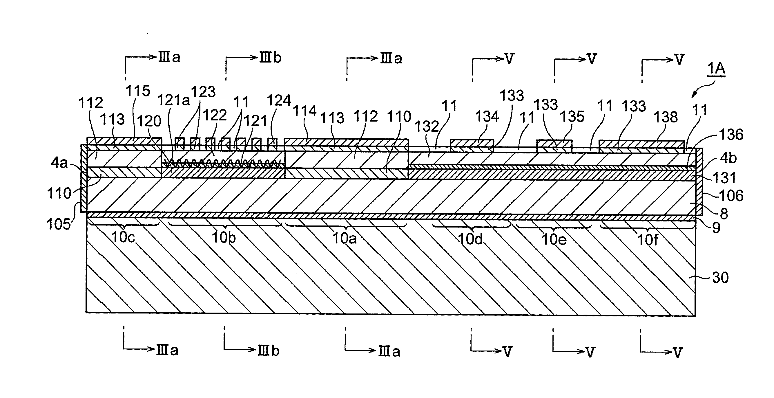
Figure 1 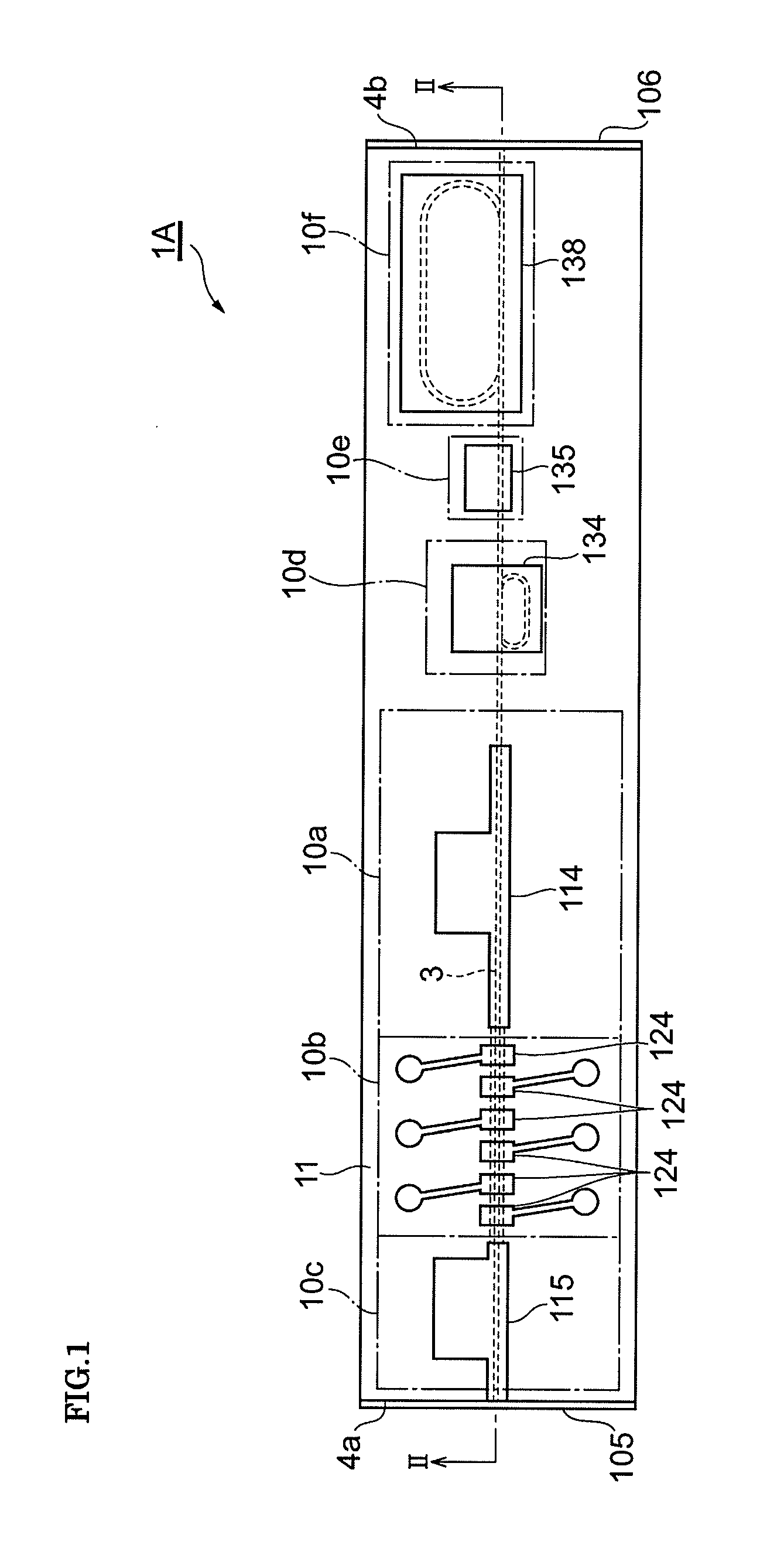
Figure 2 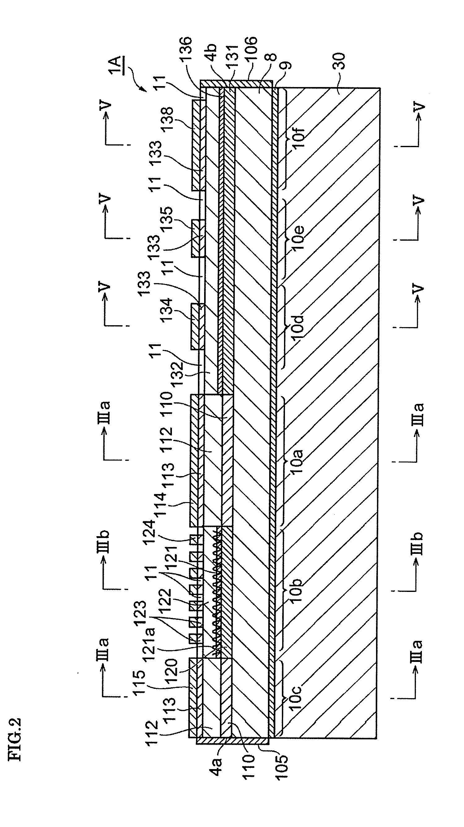
Figure 3
Abstract
Description
BACKGROUND OF THE INVENTION
[0001] 1. Field of the Invention
[0002] The present invention relates to a semiconductor laser.
[0003] 2. Description of the Related Art
[0004] Japanese Unexamined Patent Application Publication No. 2008-066318 discloses a wavelength tunable semiconductor laser. This wavelength tunable semiconductor laser includes a plurality of ring resonators having mutually different free spectral ranges (FSRs), and a gain region optically coupled to the plurality of ring resonators. More specifically, both ends of the gain region are respectively optically coupled to input ports of the individual ring resonators. Output ports of the ring resonators are optically coupled to a light emission end facet. The wavelength tunable semiconductor laser described in Japanese Unexamined Patent Application Publication No. 2008-066318 performs wavelength tuning by using vernier effect provided by the plurality of ring resonators having the mutually different FSRs.SUMMARY OF THE INVENTION[0...
Examples
Embodiment Construction
[0039]A semiconductor laser according to an embodiment of the present invention will be described in detail below with reference to the attached drawings. It is to be noted that like reference signs refer like elements when the description is given for the drawings, and redundant description is omitted.
[0040]FIG. 1 is a plan view of a semiconductor laser 1A according to the embodiment of the present invention. FIG. 2 is a cross-sectional view taken along line II-II of the semiconductor laser 1A shown in FIG. 1. The semiconductor laser 1A is a wavelength tunable semiconductor laser.
[0041]Referring to FIGS. 1 and 2, the semiconductor laser 1A includes a gain region 10a, a distributed Bragg reflector (DBR) region 10b, an amplifier region 10c, a first ring resonator region 10d, a phase adjustment region (phase adjustment portion) 10e, and a second ring resonator region 10f. These regions 10a to 10f are formed on a common semiconductor substrate 8 as shown in FIG. 2, and arranged in a pr...