
Semiconductor device and method for manufacturing the same
a technology of semiconductors and semiconductors, applied in the direction of semiconductor devices, basic electric elements, electrical equipment, etc., can solve the problems of affecting the quality of semiconductor devices, the detection is not given any consideration whatsoever, and the second resin molded body will end up being molded, so as to effectively eliminate product thickness variance, accurately position, and eliminate uneven light emission. , the effect of reducing the risk of failur
Patent Information
- Authority / Receiving Office
- US · United States
- Patent Type
- Applications(United States)
- Current Assignee / Owner
- Publication Date
- 2020-03-05
Smart Images
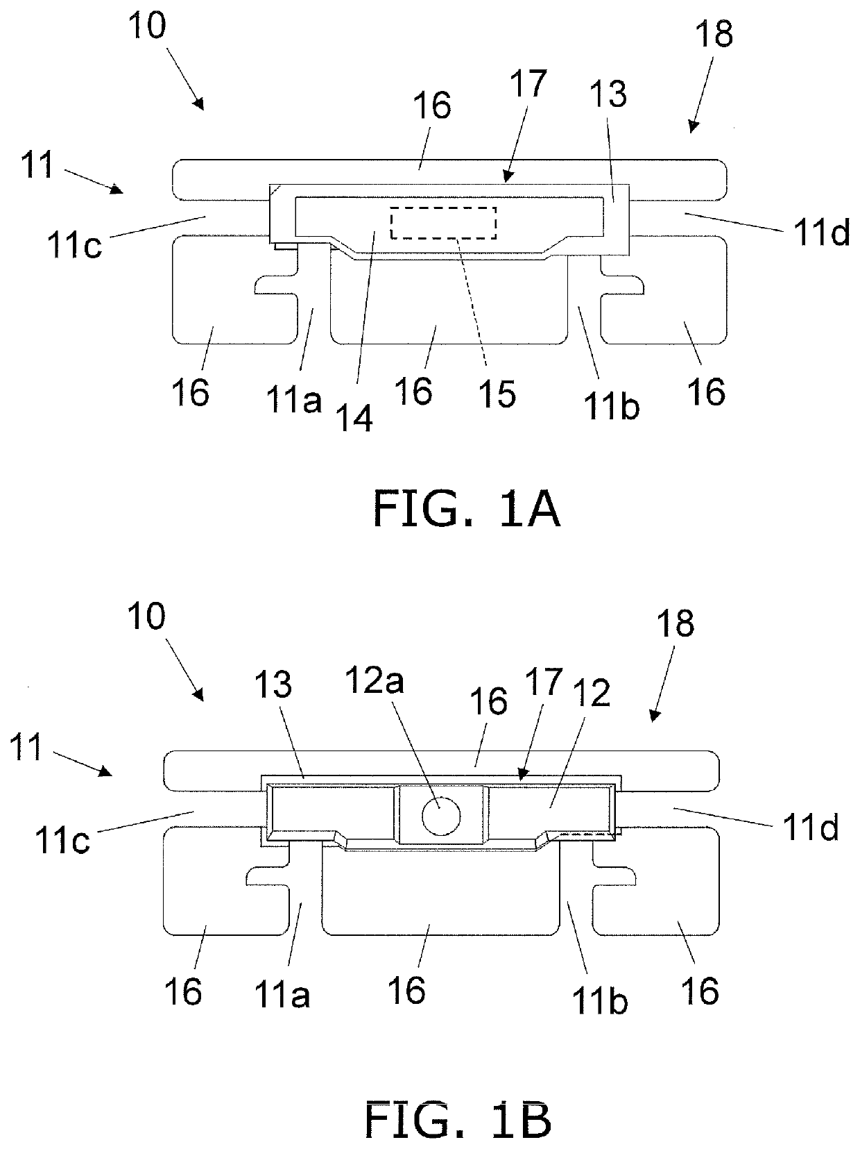
Figure 1 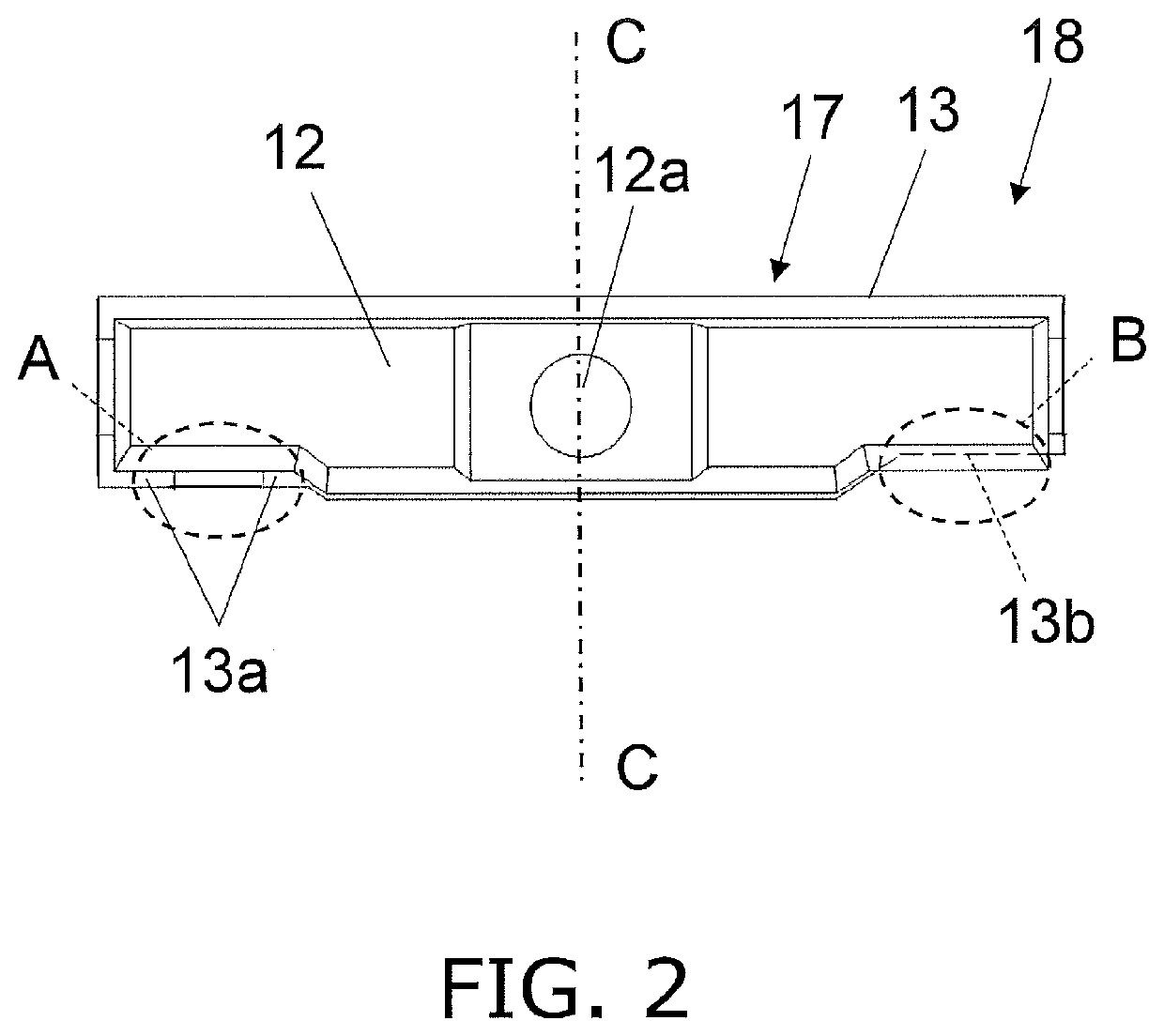
Figure 2 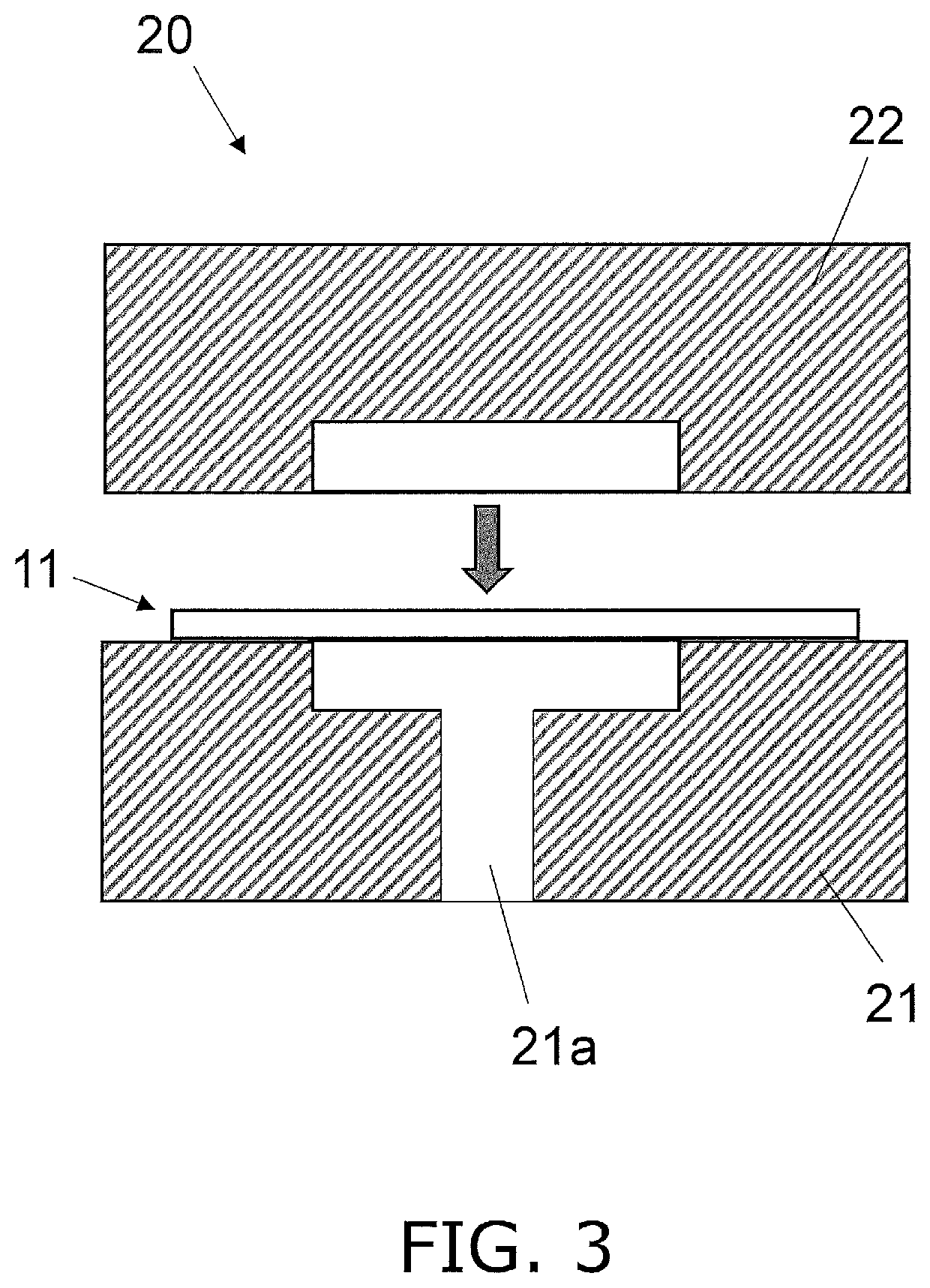
Figure 3
Abstract
Description
CROSS-REFERENCE TO RELATED APPLICATIONS
[0001] This application claims priority to Japanese Patent Application No. 2018-163380 filed on Aug. 31, 2018. The entire disclosure of Japanese Patent Application No. 2018-163380 is hereby incorporated herein by reference.BACKGROUND OF THE INVENTIONField of the Invention
[0002] The present invention relates to a semiconductor device and to a method for manufacturing the semiconductor device.Description of the Related Art
[0003] In general, a semiconductor device is manufactured by fixing a semiconductor element to a resin molded body formed by pouring a resin into a die (an upper die and a lower die) in a state in which a lead frame including a portion that will become a lead electrode is sandwiched from above and below by the dies.
[0004] In the process of manufacturing such a semiconductor device, it is important to accurately position and mold the first resin molded body and the second resin molded body disposed so as to sandwich the lead frame.[0...
Examples
embodiment 1
[0066]The semiconductor device according to an embodiment of the present invention is will now be described through reference to FIGS. 1A to 5 and FIG. 13.
[0067]The semiconductor device 10 according to the present embodiment is a light emitting device, and is a so-called side view (side light emission) type of LED (light emitting diode) having its light emitting surface on a side surface.
[0068]As shown in FIGS. 1A and 1B, the semiconductor device 10 primarily includes a semiconductor element 15 and a package 18 having two leads 11a and 11b that function as a pair of positive and negative electrodes and a resin molded body 17 that integrally holds the two leads 11a and 11b.
[0069]The resin molded body 17 has a second resin molded body 13 that is formed on the second surface (upper surface) side of the leads 11a and 11b (the lead frame 11 in the manufacturing process) and includes a portion that becomes a recess 14 that opens on a side surface, and a first resin molded body 12 that is...
embodiment 2
[0120]A semiconductor device 30 according to another embodiment of the present invention will now be described with reference to FIGS. 6A to 7B.
[0121]The semiconductor device 30 in this embodiment differs from Embodiment 1, which described a side view (side emission) type of LED in which the light emission surface is arranged on the side surface intersecting the mounting surface of the semiconductor device 10, in that it is a so-called top view (top emission) type of LED (light emitting diode) in which a semiconductor element 35 (light emitting element) is disposed on the upper surface so that the light emission surface is arranged on the opposite side of the mounting surface.
[0122]The semiconductor device 30 according to this embodiment is a light emitting device, and is a so-called top view (top emission) type of LED (light emitting diode) having the light emitting surface on its upper surface. As shown in FIGS. 6A and 6B, the semiconductor device 30 mainly includes a semiconducto...
embodiment 3
[0155]A semiconductor device 40 according to yet another embodiment of the present invention will now be described with reference to FIGS. 8A to 9B.
[0156]The semiconductor device 40 in this embodiment is the same as in Embodiment 2 in that it is a so-called top view (top emission) type of LED (light emitting diode) in which a semiconductor element 45 (light emitting element) is disposed on the upper surface. On the other hand, this embodiment differs from Embodiment 2 in that notches of different sizes are provided at two locations (above and below) of a second resin molded body 43 that is formed in left and right asymmetry around the center axis C′-C′.
[0157]The semiconductor device 40 according to this embodiment is a light emitting device, and is a so-called top view (top emission) type of LED (light emitting diode) having the light emitting surface on its upper surface. As shown in FIGS. 8A and 8B, the semiconductor device 40 mainly includes a semiconductor element 45 and a packa...