
Apparatus for cleaning semiconductor substrates
Patent Information
- Authority / Receiving Office
- US · United States
- Current Assignee / Owner
- Publication Date
- 2021-05-13
Smart Images
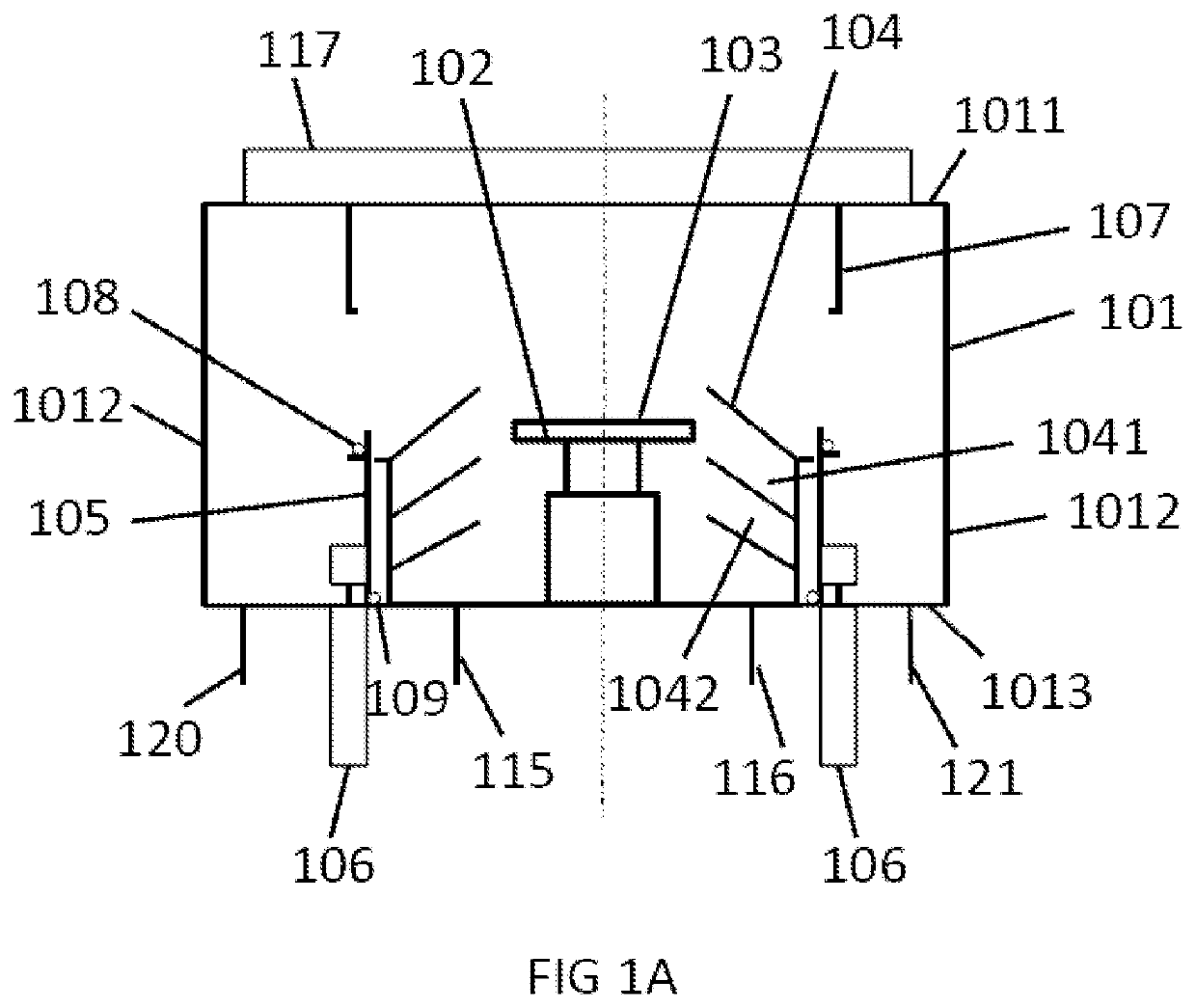
Figure 1 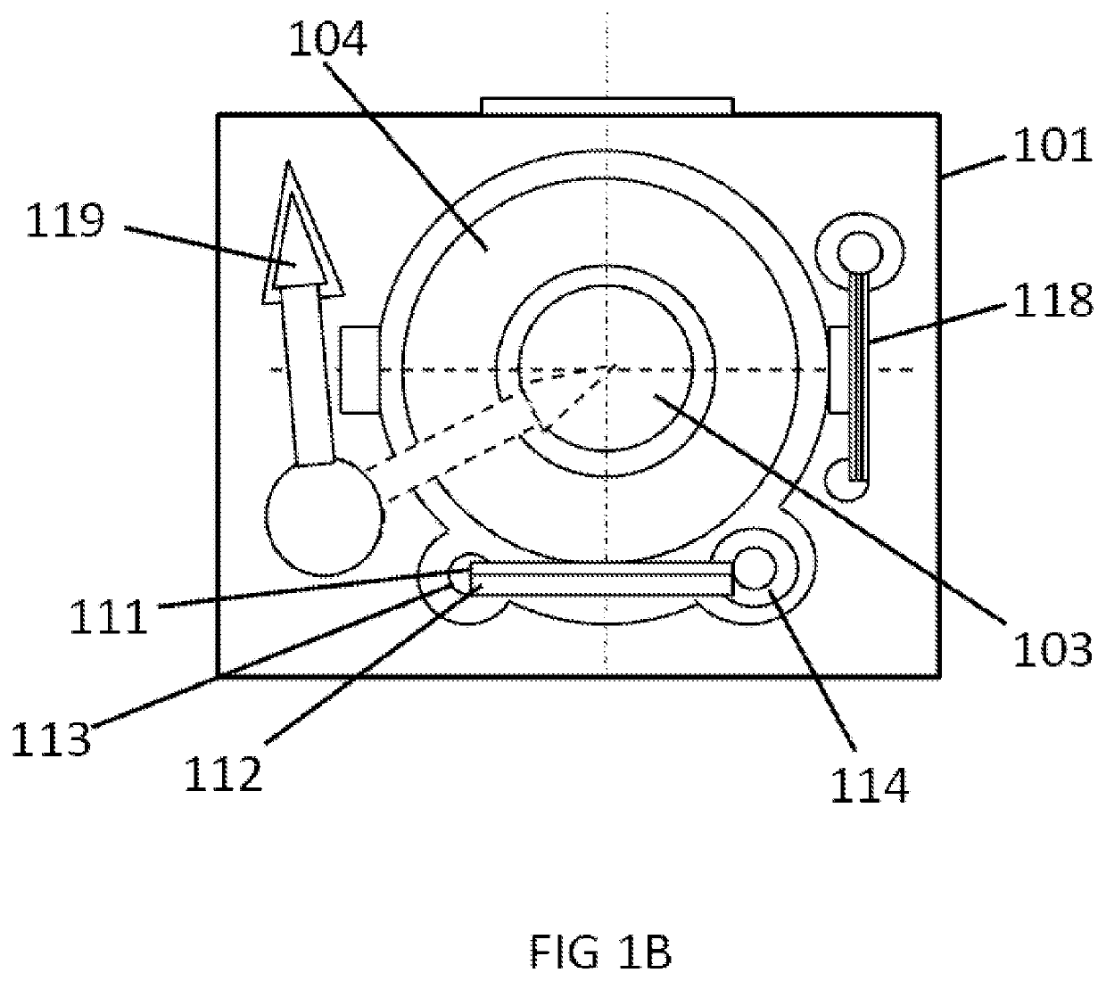
Figure 2 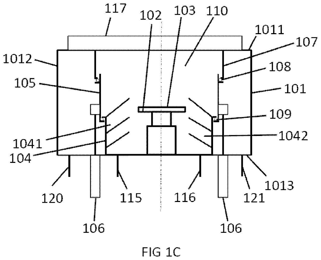
Figure 3
Abstract
Description
BACKGROUND OF THE INVENTION1. Field of the Invention
[0001] The present invention generally relates to the field of semiconductor devices manufacture, and more particularly to an apparatus for cleaning semiconductor substrates, which prevents corrosion of acid or alkali fume to parts in a cleaning chamber of the apparatus.2. The Related Art
[0002] With the development of semiconductor industry, the feature size of semiconductor devices is continuously decreasing and the integration of chips is increasing. Correspondingly, the demand to substrate surface cleanliness becomes much stricter because poor clean may cause device failure which will increase the cost of integrated circuit manufacture. For obtaining high quality semiconductor devices, the substrates must have a very clean surface, which means there are no particles, metal, organic, etc. pollutants. Although completely clean substrate surface is not present, however, the development of VLSI requires the substrate surface to be as ...
Examples
Embodiment Construction
[0013]Referring to FIG. 1A to FIG. 1D, an apparatus for cleaning semiconductor substrates according to an embodiment of the present invention is illustrated. The apparatus has a chamber 101. The chamber 101 has a top wall 1011, a side wall 1012 and a bottom wall 1013. Generally, the side wall 1012 of the chamber 101 has an opening for transferring a semiconductor substrate 103. The opening is commonly sealed by a door which is controlled to open or close. A chuck 102 is positioned in the chamber 101 for holding the semiconductor substrate 103. The chuck 102 is driven to rotate by a rotating driving device. The semiconductor substrate 103 rotates along with the chuck 102. A liquid collector 104 surrounds the chuck 102. The liquid collector 104 has at least one annular tilted trough to have spun off liquid collected therein. As an example, the liquid collector 104 has two annular tilted troughs 1041, 1042. Every annular tilted trough 1041, 1042 is connected to a pipe (not shown) throu...