
Method and apparatus for testing function of active microstructural elements and method for producing microstructural elements using the test method
a technology of active microstructural elements and test methods, applied in individual semiconductor device testing, semiconductor/solid-state device testing/measurement, instruments, etc., can solve problems such as malfunction-free elements, malfunctions that cannot be detected, and known errors that also occur during production, so as to improve test reliability and error characterization, the effect of increasing the test tim
Patent Information
- Authority / Receiving Office
- US · United States
- Patent Type
- Patents(United States)
- Current Assignee / Owner
- Publication Date
- 2008-05-20
- Estimated Expiration
- Not applicable · inactive patent
Smart Images
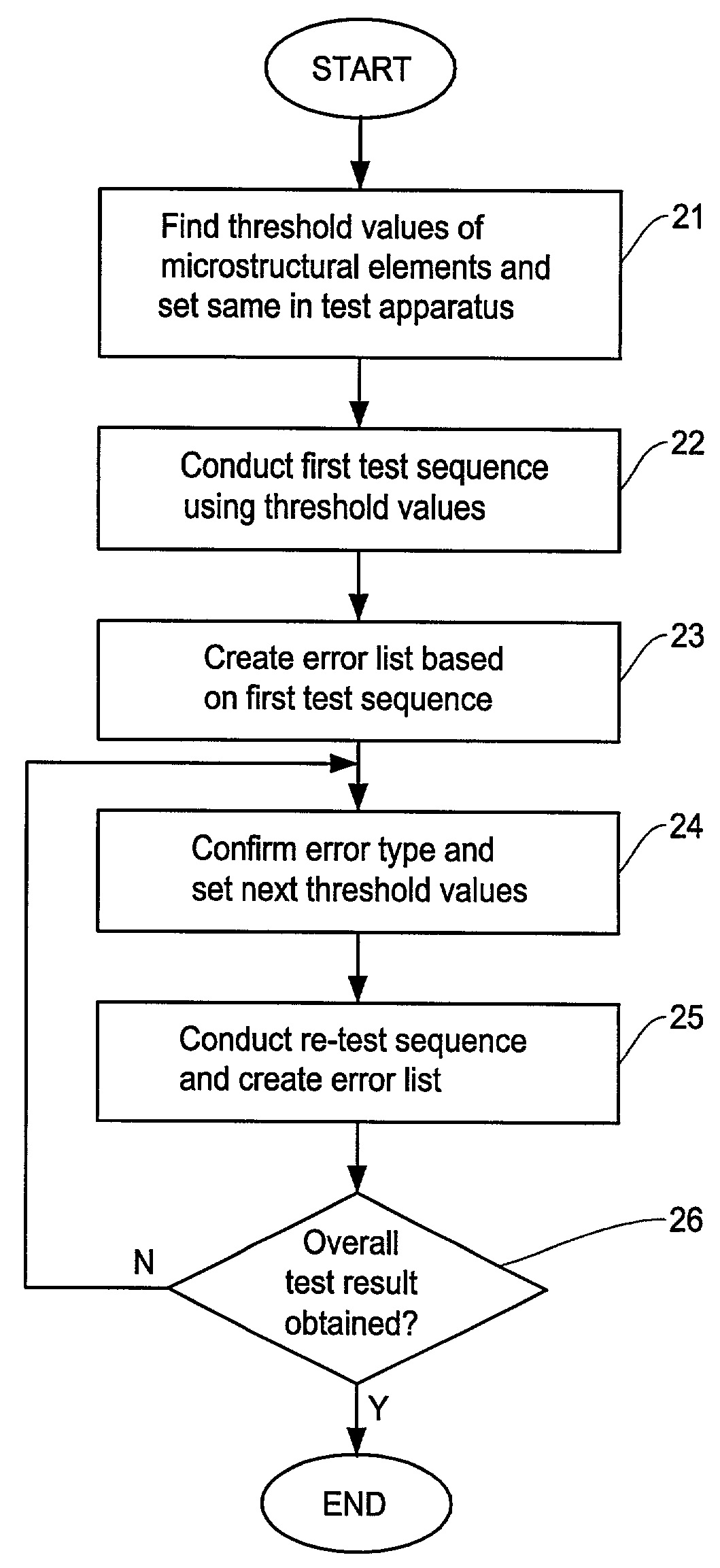
Figure 1 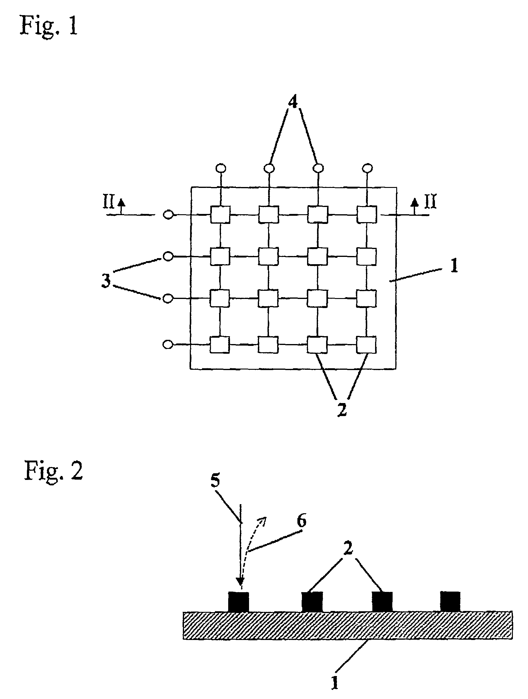
Figure 2 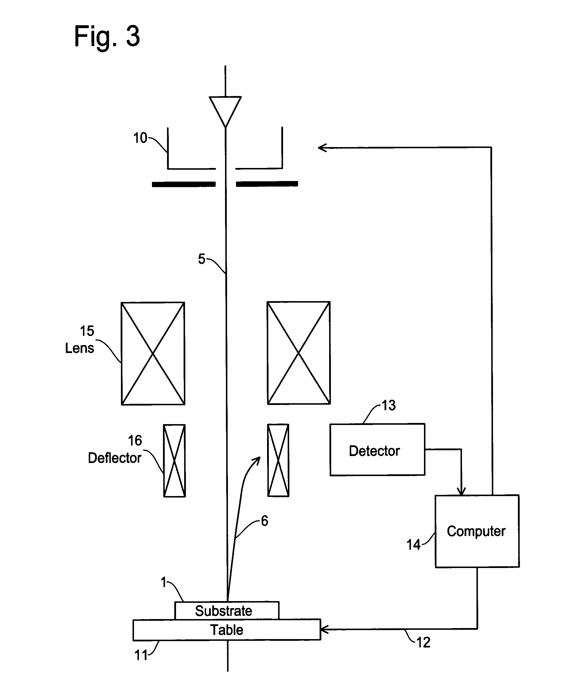
Figure 3
Abstract
Description
[0001] This is a continuation-in-part of U.S. patent application Ser. No. 09 / 482,756 filed Jan. 13, 2000 now abandoned.FIELD OF THE INVENTION
[0002] The invention relates to a method and an apparatus for testing the function of a plurality of active microstructural elements.BACKGROUND OF THE INVENTION
[0003] The term active microstructural elements is intended to refer, for example, to elements of the microelectronics sector (such as transistors, diodes, metal-insulator-metal elements), image elements and displays, electrode structures of micromechanical sensors and actuators as well as elements which emit particle radiation (for example, light or electrodes), such as laser diodes or field emission tips.
[0004] Microstructural elements of that type are produced as a plurality on a substrate, for example, wafers or glass plates. In the microstructural technology sector, mechanical, optical, electrical and other elements are produced using methods and processes which have been known for some...
Examples
Embodiment Construction
[0018]In FIGS. 1-3, a substrate 1, for example, a semiconductor wafer or liquid crystal display panel, is depicted and has a plurality of microstructural elements, the microstructural elements 2 being controllable by means of lines 3 and 4. FIG. 4 shows an operational flow of the test method of the present invention.
[0019]Possible microstructural elements include, for example, elements of the microelectronics sector (such as transistors, diodes, metal-insulator-metal elements), image elements and displays, electron structures of micromechanical sensors and actuators as well as elements (such as laser diodes or field emission tips) which emit particle radiation (for example, light or electrons). The electrical and / or mechanical properties, for example, can be tested for such microstructural elements. In addition, tests in respect of the emission properties are of interest for some microstructural elements, such as, for example, laser diodes or field emission tips.
[0020]The term elect...