
Coating/developing device and method
a technology of developing device and coating, which is applied in the direction of photosensitive materials, cleaning using liquids, instruments, etc., can solve the problems of large occupancy area, increased processing burden, and large processing space occupied by processing block, so as to suppress the deterioration of throughput, save processing block space, and efficiently use
Patent Information
- Authority / Receiving Office
- US · United States
- Patent Type
- Patents(United States)
- Current Assignee / Owner
- Publication Date
- 2013-04-02
Smart Images
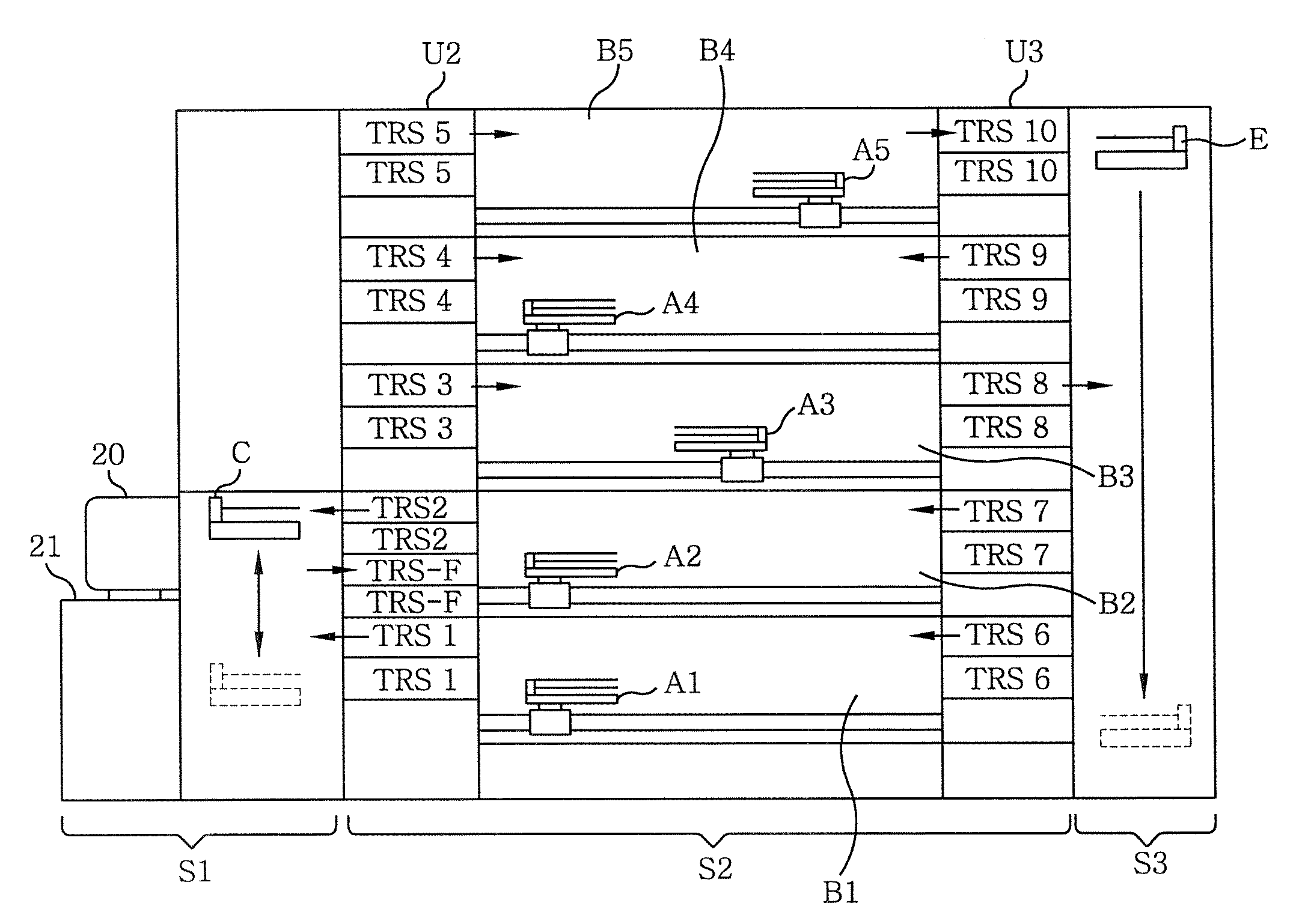
Figure 1 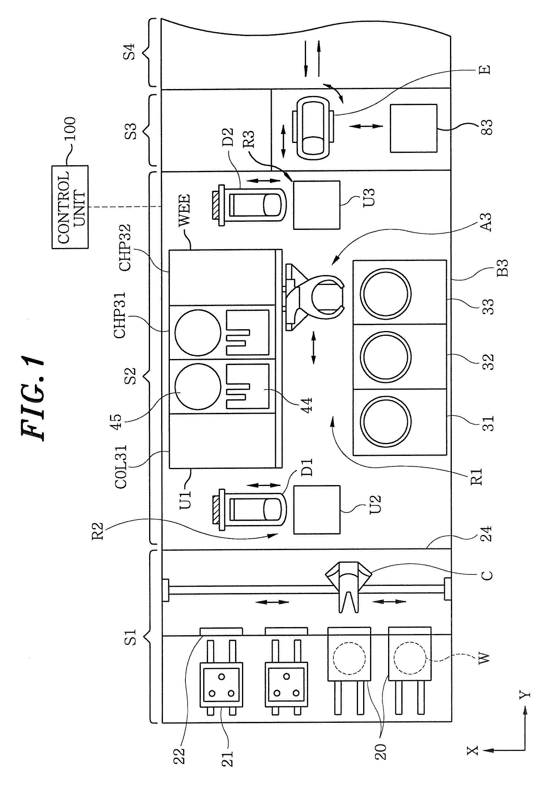
Figure 2 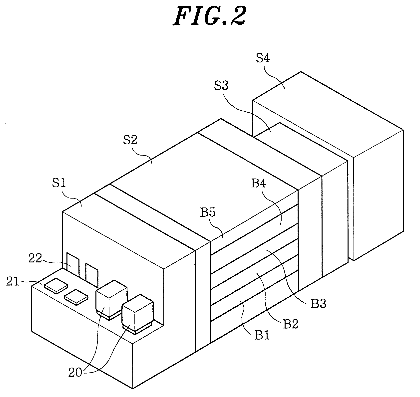
Figure 3
Abstract
Description
FIELD OF THE INVENTION
[0001] The present invention relates to a coating / developing device and method for coating a resist liquid on a substrage such as a semiconductor wafer and an LCD substrate (a glass substrate for a liquid crystal display) and developing the same after an exposure processing.BACKGROUND OF THE INVENTION
[0002] In a manufacturing process of a semiconductor device or an LCD substrate, a resist pattern is formed on a substrate by using a photolithography technology. This technology includes a series of processes of coating a resist liquid on the substrate such as a semiconductor wafer (hereinafter, referred to as ‘wafer’), forming a liquid film on the surface of the wafer, exposing the resist film by using a photo mask and then developing it.
[0003] Such processing is generally performed by using a resist pattern forming apparatus including a coating / developing device and an exposure device connected thereto as configured in, e.g., Japanese Patent Laid-open Publication N...
Examples
Embodiment Construction
[0034]Hereinafter, there will be described a coating / developing device in accordance with a first preferred embodiment of the present invention. FIG. 1 is a top view of a resist pattern forming apparatus to which the coating / developing device of the present invention is applied; FIG. 2 illustrates a schematic perspective view thereof; and FIG. 3 describes a schematic side view thereof. Such apparatus includes a carrier block S1 for loading / unloading a carrier accommodating therein, e.g., 13 wafers in a sealing state; a processing block S2 in which a plurality of, e.g., 5, unit blocks B1 to B5 are vertically arranged; an interface block S3; and an exposure device S4.
[0035]The carrier block S1 includes a mounting table 21 capable of mounting thereon a plurality of carriers 20, an opening / closing member 22 provided on a front wall as viewed from the mounting table 21 and a transfer arm C for unloading wafers W from the carrier 20 via the opening / closing member 22. The transfer arm C is...