
Data transfer apparatus and image forming system
a data transfer and image forming technology, applied in the field of data transfer apparatus and image forming system, can solve the problems of reducing the throughput of transferring data of some kinds of transactions via a virtual channel, affecting the quality of data transfer, and reducing the communication quality of data transfer stream, so as to improve the throughput of transferring data and increase the cost or power consumption
Patent Information
- Authority / Receiving Office
- US · United States
- Patent Type
- Patents(United States)
- Current Assignee / Owner
- Publication Date
- 2014-06-03
- Estimated Expiration
- Not applicable · inactive patent
Smart Images
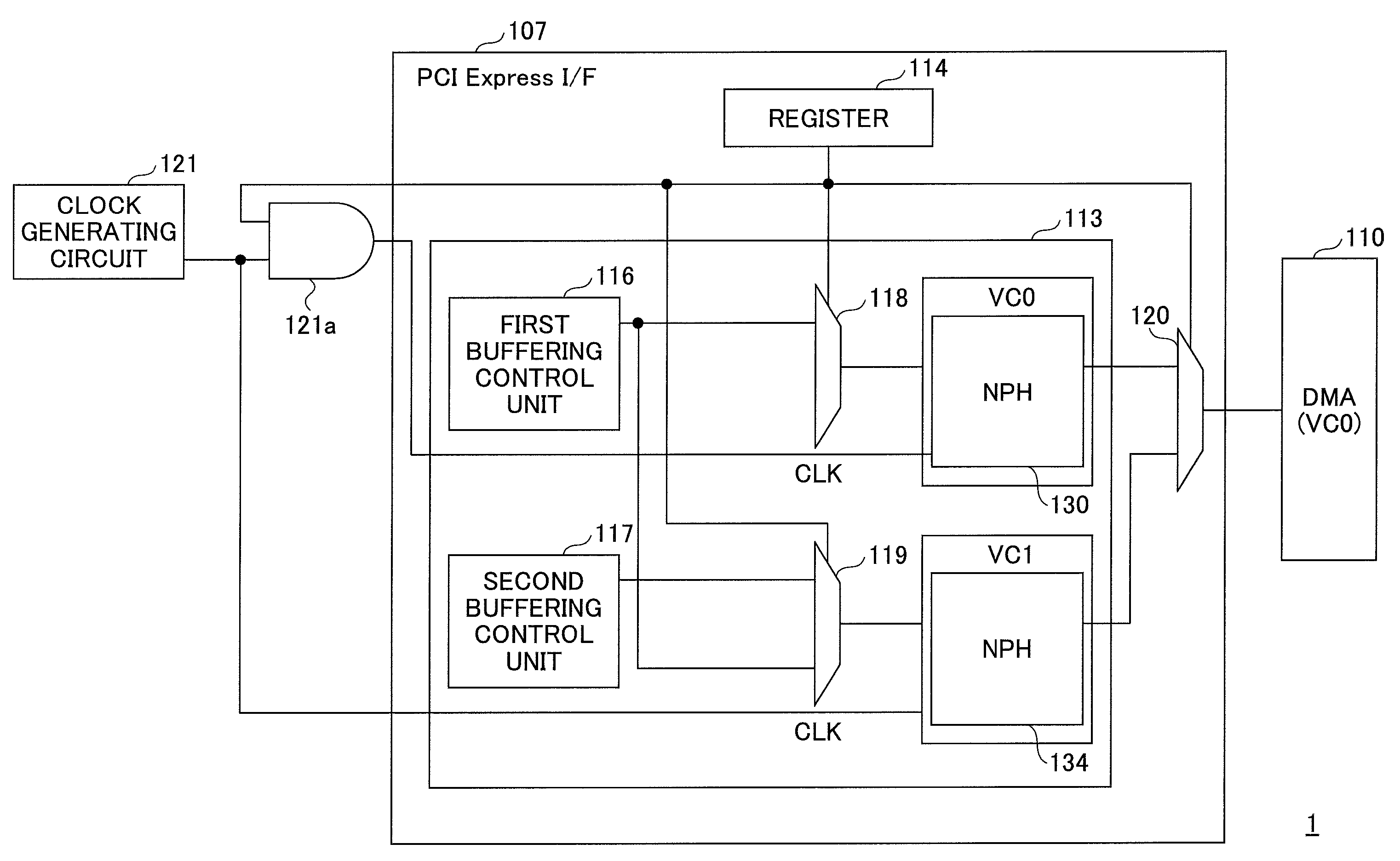
Figure 1 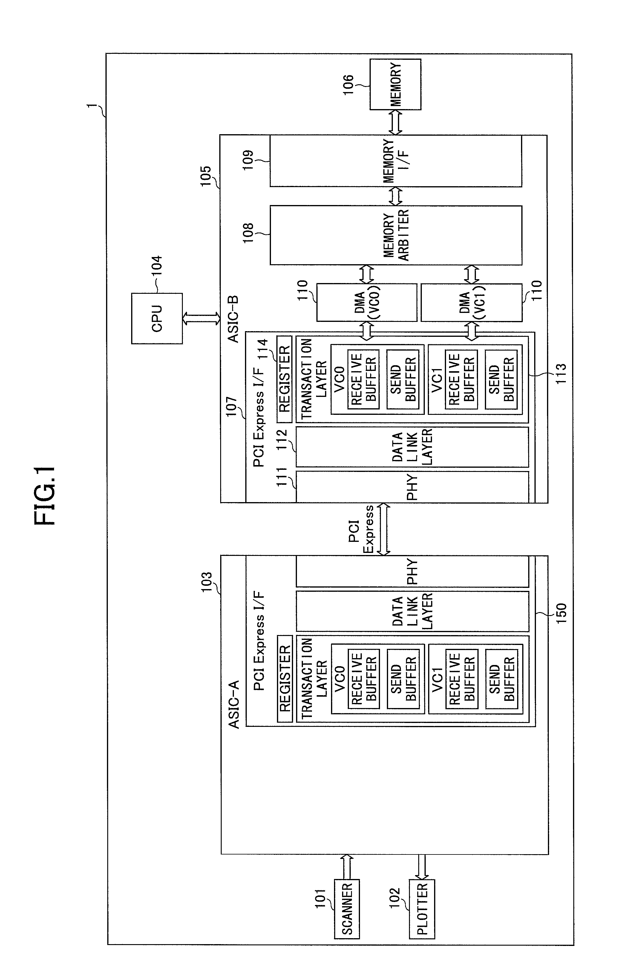
Figure 2 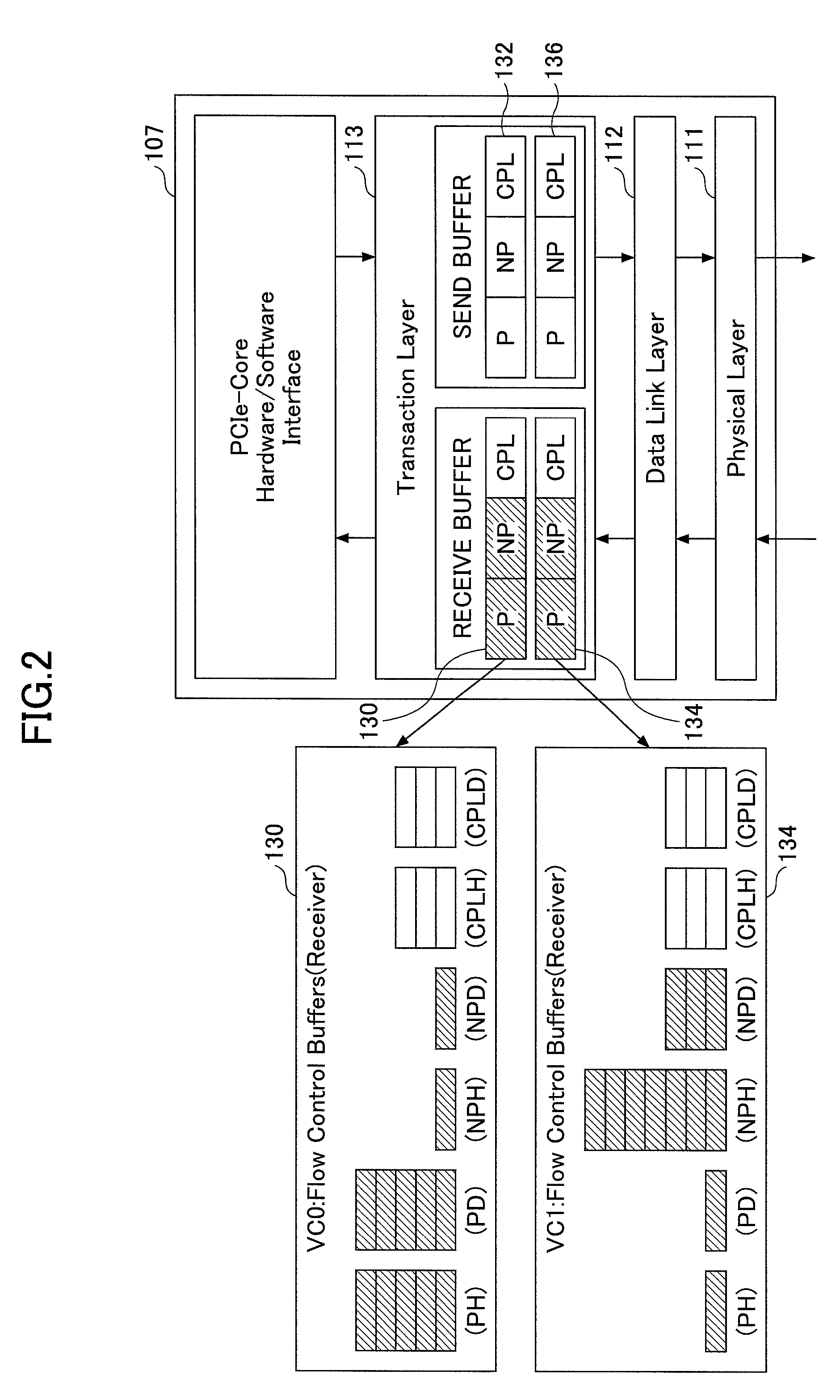
Figure 3
Abstract
Description
BACKGROUND OF THE INVENTION
[0001] 1. Field of the Invention
[0002] The present invention relates to a data transfer apparatus and an image forming system.
[0003] 2. Description of the Related Art
[0004] Recently, a high speed serial transmission line, whose transmission speed exceeds several Gbps, capable of transmitting data much faster than Ethernet (registered trademark) has been actualized. For this kind of transmission line, a standard of a local In / Out (I / O) adopting a communication method similar to a conventional computer network has been spreading. Thus, a data network for communications within a chip, between chips or between boards of a Large Scale Integration (LSI) by packet communication using a serial transmission line and a switch, similar to the computer network, is becoming to be used in an electric device to be embedded in a system.
[0005] Specifically, for a system such as a Personal Computer (PC) system, an embedded system such as an image forming apparatus such as a Mult...
Examples
first embodiment
System Structure
[0055]FIG. 1 is a block diagram showing an example of a structure of a PCI Express system of the embodiment which is embedded in a MFP 1 as an example of an embedded system.
[0056]The MFP 1 of the embodiment includes a scanner 101, a plotter 102, a CPU 104, a memory 106, a controller-side ASIC-B 105 and an opposite ASIC. In FIG. 1, an example where the opposite ASIC is an opposite ASIC-A 103 is shown.
[0057]The scanner 101 corresponds to an image reading unit that optically reads a document set at a reading surface of the MFP 1 to form image data. In other words, the scanner 101 is an example of an image input engine. The image data is input by the scanner 101 to be stored (written) in the memory 106.
[0058]The plotter 102 corresponds to an image writing unit that prints a bitmap image of image data read from the memory 106 on a paper or the like by an electro-photographic process, for example. In other words, the plotter 102 is an example of an image output engine.
[005...
second embodiment
[0112]In the first embodiment, an example where the connections to the receive buffers (flow control buffers) of the transaction layer 113 of the PCI Express I / F 107 of the controller-side ASIC-B 105 as the receiver-side (Rx side) are switched on and off is explained. Specifically, as the receive buffer “NPH” of the first virtual channel VC0 is optimized for the MFP 1, the corresponding capacity is set very small. On the other hand, the receive buffer “NPH” of the second virtual channel VC1 is set to have larger capacity as the receive buffer “NPH” of the second virtual channel VC1 is also optimized for the MFP 1. Thus, when the data related to the memory read request is supposed to be transmitted via the first virtual channel VC0, the receive buffer “NPH” of the second virtual channel VC1 is used instead of the receive buffer “NPH” of the first virtual channel VC0. In other words, even for the data transmission by the first virtual channel VC0, the receive buffer “NPH” of the secon...