
Semiconductor device comprising oxide semiconductor
a semiconductor and semiconductor technology, applied in the direction of semiconductor devices, electrical apparatus, transistors, etc., can solve the problems of reducing the yield of transistors in the manufacturing process, and achieve the effects of high yield, excellent electrical characteristics, and high reliability
Patent Information
- Authority / Receiving Office
- US · United States
- Patent Type
- Patents(United States)
- Current Assignee / Owner
- Publication Date
- 2016-03-15
Smart Images
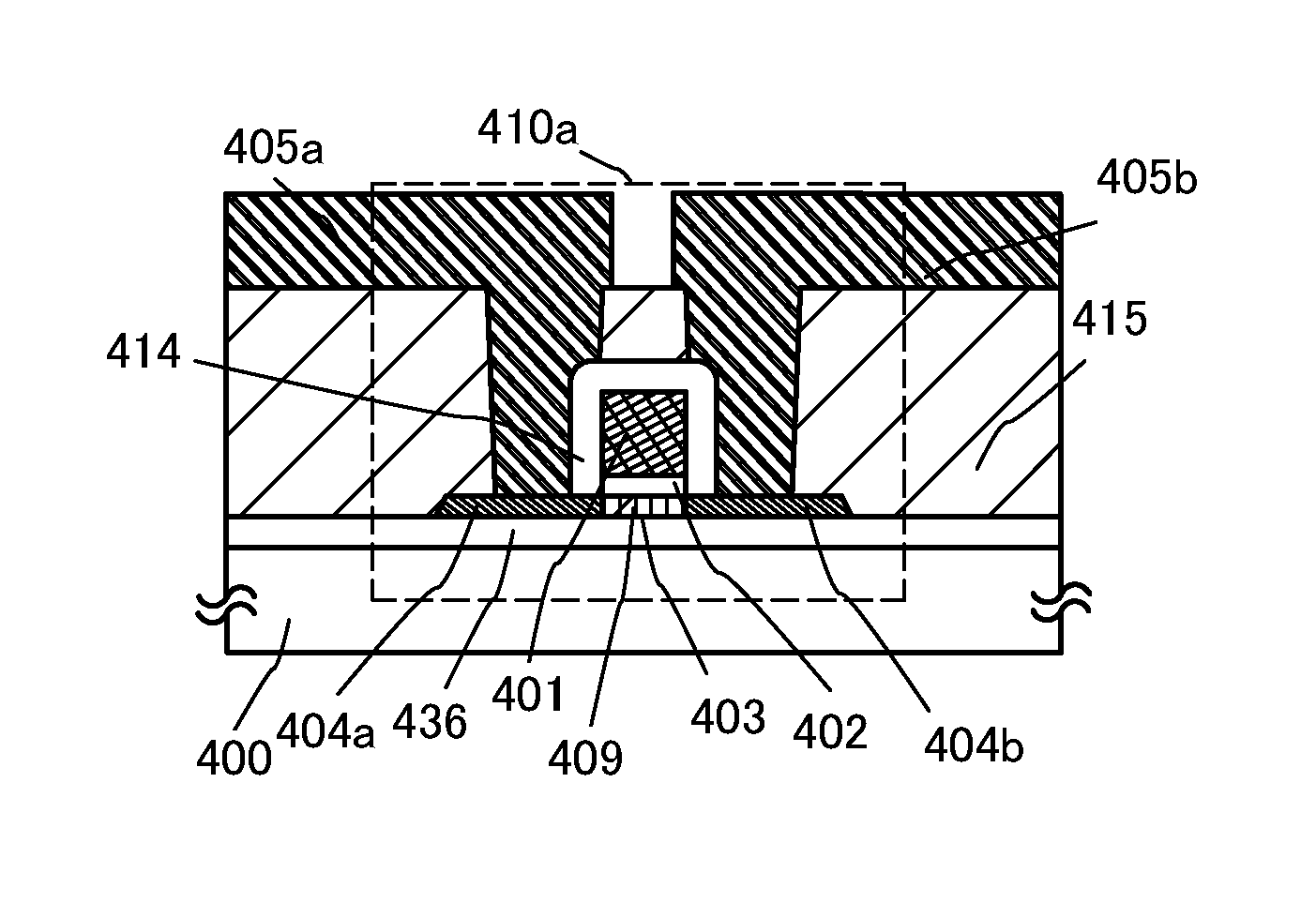
Figure 1 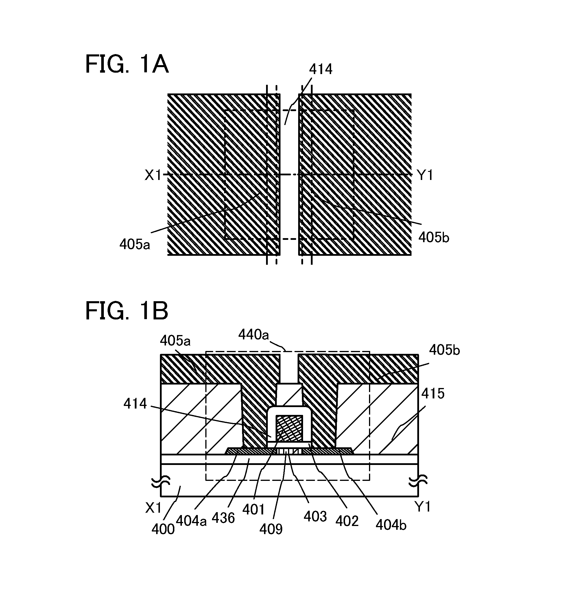
Figure 2 
Figure 3
Abstract
Description
BACKGROUND OF THE INVENTION
[0001] 1. Field of the Invention
[0002] The present invention relates to a semiconductor device and a method for manufacturing the semiconductor device.
[0003] In this specification, a semiconductor device generally means any device which can function by utilizing semiconductor characteristics, and an electro-optic device, a semiconductor circuit, and an electronic appliance are all included in the category of the semiconductor device.
[0004] 2. Description of the Related Art
[0005] Attention has been focused on a technique for forming a transistor using a semiconductor thin film (also referred to as a thin film transistor (TFT)) formed over a substrate having an insulating surface. The transistor is applied to a wide range of electronic devices such as an integrated circuit (IC) or an image display device (display device). A silicon-based semiconductor material is widely known as a material for a semiconductor thin film applicable to a transistor. As another mater...
Examples
embodiment 1
[0046]In this embodiment, one embodiment of a semiconductor device and a method for manufacturing the semiconductor device will be described with reference to FIGS. 1A and 1B. In this embodiment, a transistor including an oxide semiconductor film is described as an example of the semiconductor device.
[0047]The transistor may have a single-gate structure in which one channel formation region is formed, a double-gate structure in which two channel formation regions are formed, or a triple-gate structure in which three channel formation regions are formed. Alternatively, the transistor may have a dual-gate structure including two gate electrode layers positioned over and under a channel formation region with a gate insulating film provided therebetween.
[0048]A transistor 440a illustrated in FIGS. 1A and 1B is an example of a top-gate transistor. FIG. 1A is a plan view and FIG. 1B is a cross-sectional view taken along dashed line X1-Y1 in FIG. 1A. Note that in FIG. 1A, an interlayer ins...
embodiment 2
[0190]In this embodiment, another embodiment of a semiconductor device and a method for manufacturing the semiconductor device will be described with reference to FIGS. 5A to 5C. The same portion as or a portion having a function similar to those in the above embodiment can be formed in a manner similar to that described in the above embodiment, and also the steps similar to those in the above embodiment can be performed in a manner similar to that described in the above embodiment, and repetitive description is omitted. Thus, the descriptions thereof are not repeated in this embodiment.
[0191]Transistors 430a and 430b illustrated in FIGS. 5A to 5C are examples of a top-gate transistor. FIG. 5A is a plan view of the transistor 430a and FIG. 5B is a cross-sectional view taken along dashed line X2-Y2 in FIG. 5A. Note that in FIG. 5A, the interlayer insulating film 415 is not illustrated. FIG. 5C is a cross-sectional view of the transistor 430b.
[0192]As illustrated in FIGS. 5B and 5C, ...
embodiment 3
[0218]In this embodiment, an example of a semiconductor device which includes the transistor described in this specification, which can hold stored data even when not powered, and which does not have a limitation on the number of write cycles, will be described with reference to drawings.
[0219]FIGS. 6A to 6C illustrate an example of the structure of a semiconductor device. FIGS. 6A to 6C illustrate a cross-sectional view, a plan view, and a circuit diagram, respectively, of the semiconductor device. Here, FIG. 6A corresponds to cross sections taken along line C1-C2 and line D1-D2 in FIG. 6B.
[0220]The semiconductor device illustrated in FIGS. 6A and 6B includes a transistor 160 including a first semiconductor material in a lower portion, and a transistor 162 including a second semiconductor material in an upper portion. The structure of the transistor described in Embodiment 1 or Embodiment 2 can be applied to the transistor 162. This embodiment shows an example where the structure o...