
Lithography methods, and elements and devices obtainable by the methods
The introduction of novel metal-organic complexes for EUV resist materials addresses the challenges of sensitivity, line edge roughness, and resolution in existing EUV resist materials, achieving low-dose patterning with high resolution and improved stability for industrial-scale production.
Patent Information
- Application Number
- PCT/FI2024/050573
- Authority / Receiving Office
- WO · WO
- Patent Type
- Applications
- Current Assignee / Owner
- Priority Date
- 2024-10-25
- Filing Date
- 2024-10-25
- Publication Date
- 2025-05-08
AI Technical Summary
Existing EUV resist materials face challenges such as trade-offs between sensitivity, line edge roughness, and resolution, and have inadequate shelf-life stability, limiting their use in industrial-scale production.
The development of novel metal-organic complexes with a first metal chelating moiety and a second polymerizable, organic moiety, which are used to form resist films that can be patterned using electron beam or light radiation, and developed with specific developers to improve throughput.
The new resist materials enable low-dose patterning with high resolution, improved shelf-life stability, and enhanced sensitivity, addressing the limitations of current EUV resist materials and improving industrial-scale production capabilities.
Smart Images
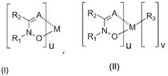
Figure IMGF000004_0001 
Figure IMGF000005_0001 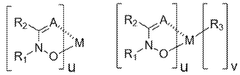
Figure IMGF000007_0001
Abstract
Description
[0001] Lithography methods, and elements and devices obtainable by the methods
[0002] Technical Field
[0003] The present invention relates to radiation sensitive metal-organic complexes usable in lithography methods and methods of preparation of elements and devices using the methods. In particular, the invention concerns functional solution processable organo / poly-metallic electron or photo resist complexes, metal-organic and organopoly-metal-complex compositions, and polymers thereof useful for coating of semiconductors and optical substrates and for forming metal oxide films, and in particular the methods concern the use of one or more developers.
[0004] Background
[0005] Advanced lithography methods which use electron beam or extreme ultraviolet light (EUV) as the radiation source have been of great interest due to their capabilities of patterning at sub-10 nm resolution. However, existing EUV resist materials still face many challenges and there is generally a trade-off between sensitivity (S), line edge roughness (L), and resolution (R).
[0006] Presently, chemically amplified resists (CAR) are utilized to increase sensitivity. The CAR’s mainly consist of a main polymeric or molecular component as a matrix, photoacid generator molecules, and base quencher molecules. Upon irradiation, the photo-acid generator molecules (PAGs) interact with the light to generate acids; then a change in dissolution rate of the matrix begins during a subsequent postexposure bake (PEB) step. During this step reactions of specific groups of the matrix are catalyzed by the photogenerated acid molecules changing hydrophilicity, or inducing crosslinking or back bone scission, and hence alter solubility in developers, such as aqueous base developers.
[0007] A considerable disadvantage of present CAR’s is acid diffusion that can cause a large stochastic effect which leads to undesired bridging between patterns, hydrodynamic radii of polymers in CAR, making it inherently difficult to accomplish a sub-10 nm feature size. The root-mean-square end-to-end distance for polymer chains in conventional CAR photoresists ranges from 6 to 10 nm and the presence of additives could, in fact, lead to an increase in defects.
[0008] Non-CAR compositions, which utilize metal clusters or metal complexes, avoid some of the disadvantages of CAR’s but still have inadequate shelf-life stability due to the presence of environmentally susceptible or moisture sensitive functionalities / functional groups that limit the use of the materials for industrial scale production.
[0009] It is an aim of the present invention to address at least some of these problems by providing new resist materials and lithography methods. A particular aim of the present invention is to provide a method of lithography patterning which includes the selection of appropriate developer to improve or adjust throughput.
[0010] Summary
[0011] This Summary is provided to introduce a selection of concepts in a simplified form that are further described below in the Detailed Description. This Summary is not intended to identify key features or essential features of the claimed subject matter, nor is it intended to be used to limit the scope of the claimed subject matter.
[0012] It is an object of the present invention to provide lithography methods useful in optical lithography applications. The present invention relates to lithography methods utilizing metal-organic complexes which have a first metal chelating moiety and a second polymerizable, organic moiety. The present invention also provides the use of the novel complexes as well as oligo- and polymers thereof for forming layers and films, such as metal oxide layers and films, in particular in lithographic applications.
[0013] It is another object of the present invention to provide an optical element, optically active device or optical or semiconductor device obtainable by a method as defined in the present disclosure.
[0014] In one aspect is provided a lithography method comprising: i) applying an organometallic compound represented by Formula (I) or Formula (II), or a polymer obtained by subjecting one or more compounds represented by Formula (I) and / or Formula (II) to conditions of polymerization, optionally in the presence of oxygen, or a composition comprising the organometallic compound represented by Formula (I) or Formula (II), and / or the polymer, for a resist on a substrate, wherein
[0015] M stands for a metal, in particular a transition metal, a non-metal or a metalloid of groups 1 to 15;
[0016] Ri stands for hydrogen or an optionally substituted hydrocarbyl residue;
[0017] R2 stands for hydrogen, a hydrocarbyl residue of a saturated or unsaturated, linear, branched or cyclic hydrocarbon, optionally substituted with one or more reactive or non-reactive groups optionally containing heteroatoms;
[0018] R3 stands for an alkenyl group with 2 to 10 carbon atoms, said alkenyl being optionally substituted with one or more alkyl groups having 1 to 10 carbon atoms; an acrylate, methacrylate, carbamate, thiocarbamate, thiacarbamate or acetate, or
[0019] R3 represents a residue corresponding to the structure placed within the lefthand side brackets of Formula (II), whereby R1 stands for hydrogen or an optionally substituted hydrocarbyl residue and R2 stands for hydrogen, a hydrocarbyl residue or a saturated or unsaturated, linear, branched or cyclic hydrocarbon, optionally substituted with one or more reactive or non-reactive groups optionally containing heteroatoms, at least one of said substituents R1 and R2 in the meaning of R3 being different from the corresponding substituents of the structure placed within the left-hand side brackets of Formula (II);
[0020] A stands for a heteroatom; and u and v are independently selected from integers having a value in the range from 1 to 10; thereby forming a resist film on the substrate; ii) exposing the formed resist film to light or electron beam radiation, thereby forming an exposed resist film on the substrate; and iii) developing the formed exposed resist film with one or more developers, thereby forming a patterned resist film on the substrate; wherein the one or more developers are each independently selected from the group of compounds represented by Formula (VIII), Formula (IX), Formula (X), Formula (XI), and Formula (XII), wherein R , Rn, R12, R13, R14, and R15 are each independently selected from linear and branched hydrocarbon groups having 1 to 10 carbon atoms; and R and R17 are each independently selected from H, linear and branched hydrocarbon groups having 1 to 10 carbon atoms, linear and branched alkoxy groups having 1 to 10 carbon atoms, and halogen.
[0021] It is another object of the present invention to provide an optical element, optically active device or optical or semiconductor device obtainable by a method as defined in the present disclosure.
[0022] In one aspect is provided an optical element, optically active device or optical or semiconductor device obtainable by a method as defined in the present disclosure.
[0023] Further features and advantages of the present technology will appear from the following detailed description. The objects of the invention are achieved by lithographic methods and optical elements, optically active devices or optical or semiconductor devices obtainable by a method as defined in the present disclosure that are characterized by what is stated in the independent claims. Preferred embodiments of the invention are disclosed in the dependent claims.
[0024] Brief Description of the Drawings
[0025] Figure 1 show in sideview schematically the principal steps of forming a trilayered lithography stack;
[0026] Figure 2 shows the NMR spectra of a novel functional metal-hydroxamate according to the invention comprising of a metal-oxygen bond adjacent to the nitrogen in one moiety with a polymerizable / cross-linkable group (methacrylate) in another moiety of the complex of Example 1 ;
[0027] Figure 3 shows the applicability of the present invention in a 4-layered structure comprising a photoresist layer 120 on top a Silicon hard mask Si-BARC or Silicon oxynitride or metal oxides 130 and SOC or Chemical Vapor Deposition (CVD) or ALD carbon or high temperature SOC 140 layers, which are deposited upon a substrate 150;
[0028] Figure 4 shows the exposer of newly developed material / photoresist layer under 250 nm lamp;
[0029] Figure 5 shows the SEM after electron-beam radiation exposer on a functional metal-hydroxamate film prepared according to Example 1 at a dose of 150 pC / cm2and developing using NBA for 30 s;
[0030] Figure 6 shows the SEM after electron-beam radiation exposer on a functional metal-hydroxamate film prepared according to Example 1 at a dose of 150 pC / cm2and developing using NBA for 30 s;
[0031] Figure 7 shows the SEM after electron-beam radiation exposer on a functional metal-hydroxamate film prepared according to Example 1 at a dose of 500 pC / cm2and developing using PGMEA for 30 s;
[0032] Figures 8a-c show the SEM after electron-beam radiation exposer on a functional metal-hydroxamate film prepared according to Example 1 at a dose of 150 pC / cm2and developing using NBA for 45 s (Figure 8a); at a dose of 450 pC / cm2and developing using 2-heptanone for 20 s (Figure 8b); and at a dose of 500 pC / cm2and developing using PGMEA for 30 s (Figure 8c); and
[0033] Figure 9a-c show the SEM after electron-beam radiation exposer on a functional metal-hydroxamate film prepared according to Example 1 at a dose of 350 pC / cm2and developing using 2-heptanone for 15+5 s (Figure 9a); at a dose of 700 pC / cm2and developing using 2-heptanone for 20+5 s (Figure 9b); and at a dose of 800 pC / cm2and developing using 2-heptanone for 25+5 s (Figure 9c).
[0034] Detailed description
[0035] Unless otherwise stated herein or clear from the context, any percentages referred to herein are expressed as percent by weight based on a total weight of the respective composition.
[0036] Molecular weight is expressed as weight average molecular weight.
[0037] Unless otherwise stated, properties that have been experimentally measured or determined herein have been measured or determined at room temperature. Unless otherwise indicated, room temperature is 25 °C. It must also be noted that, as used in the specification and the appended claims, the singular forms “a,” “an” and “the” include plural referents unless otherwise specified.
[0038] As used herein, the term “about” refers to a value which is ± 5 % of the stated value. As used herein, the term “about” refers to the actual given value, and also to an approximation to such given value that would reasonably be inferred to one of ordinary skill in the art, including approximations due to the experimental and / or measurement conditions for such given value.
[0039] As used herein, the structure of complex obtained by using nuclear magnetic resonance using dimethyl sulfoxide as a reference.
[0040] The resist films were exposed to electron beam lithography using Raith EBPG 5200 system. SEM images are taker by Zeiss Supra 35.
[0041] As used herein and hereafter, “HP” refers to half-pitch.
[0042] In one aspect is provided a lithography method comprising: i) applying an organometallic compound represented by Formula (I) or Formula (II), or a polymer obtained by subjecting one or more compounds represented by Formula (I) and / or Formula (II) to conditions of polymerization, optionally in the presence of oxygen, or a composition comprising the organometallic compound represented by Formula (I) or Formula (II), and / or the polymer, for a resist on a substrate,
[0043] (I) (H) wherein
[0044] M stands for a metal, in particular a transition metal, a non-metal or a metalloid of groups 1 to 15;
[0045] Ri stands for hydrogen or an optionally substituted hydrocarbyl residue; R2 stands for hydrogen, a hydrocarbyl residue of a saturated or unsaturated, linear, branched or cyclic hydrocarbon, optionally substituted with one or more reactive or non-reactive groups optionally containing heteroatoms;
[0046] R3 stands for an alkenyl group with 2 to 10 carbon atoms, said alkenyl being optionally substituted with one or more alkyl groups having 1 to 10 carbon atoms; or an acrylate, methacrylate, carbamate, thiacarbamate or acetate, or R3 represents a residue corresponding to the structure placed within the lefthand side brackets of Formula (II), whereby R1 stands for hydrogen or an optionally substituted hydrocarbyl residue and R2 stands for hydrogen, a hydrocarbyl residue or a saturated or unsaturated, linear, branched or cyclic hydrocarbon, optionally substituted with one or more reactive or non-reactive groups optionally containing heteroatoms, at least one of said substituents R1 and R2 in the meaning of R3 being different from the corresponding substituents of the structure placed within the left-hand side brackets of Formula (II);
[0047] A stands for a heteroatom; and u and v are independently selected from integers having a value in the range from 1 to 10; thereby forming a resist film on the substrate; ii) exposing the formed resist film to light or electron beam radiation, thereby forming an exposed resist film on the substrate; and iii) developing the formed exposed resist film with one or more developers, thereby forming a patterned resist film on the substrate; wherein the one or more developers are each independently selected from the group of compounds represented by Formula (VIII), Formula (IX), Formula (X), Formula (XI), and Formula (XII), wherein R10, R11, R12, R13, R14, and R15 are each independently selected from linear and branched hydrocarbon groups having 1 to 10 carbon atoms; and R and R17 are each independently selected from H, linear and branched hydrocarbon groups having 1 to 10 carbon atoms, linear and branched alkoxy groups having 1 to 10 carbon atoms, and halogen.
[0048] Alternatively, in i), applying a polymer represented by Formula (III)
[0049] (III), or a composition comprising the polymer represented by Formula (III), for a resist on a substrate, wherein each R2’ stands for hydrogen, a hydrocarbyl residue of a saturated or unsaturated, linear, branched or cyclic hydrocarbon, optionally substituted with one or more reactive or non-reactive groups optionally containing heteroatoms; w is an integer having a value in the range from 100 to 100,000; and
[0050] Ri, A, and M are as defined in the present disclosure, thereby forming a resist film on the substrate.
[0051] Additionally, or alternatively, in iii), developing the formed exposed resist film with one or more developers is developing the formed exposed resist film with a developer composition comprising one or more developers, thereby forming a patterned resist film on the substrate.
[0052] Additionally, or alternatively, in i), applying a polymer obtained by subjecting the one or more compounds represented by Formula (I) and / or Formula (II) to conditions of polymerization in the presence of oxygen, for example to conditions of radical polymerization, optionally in the presence of cross-linkable monomers to obtain copolymers.
[0053] Additionally, or alternatively, in i), applying a polymer obtained by subjecting the one or more compounds represented by Formula (I) and / or Formula (II) to conditions of polymerization in the presence of oxygen, for example to conditions of radical polymerization, optionally in the presence of cross-linkable monomers to obtain copolymers, wherein the polymer being represented by Formula (I I lb):
[0054] (lllb), or a composition comprising the polymer represented by Formula (lllb), for a resist on a substrate, wherein x is an integer having a value in the range from 1 to 100; and each Ri, R2, A, and M, are as defined in the present disclosure.
[0055] Additionally, or alternatively, in i), applying a composition comprising the organometallic compound represented by Formula (I) and the organometallic compound represented by Formula (II), and / or the polymer.
[0056] Additionally, or alternatively, the method is free of a photoacid and / or a photo-base generator. Additionally, or alternatively, the photoacid generator is selected from commonly known photoacid generators such as, but not limited to, salts formed by combinations of triarylsulfonium and diaryliodonium cations, and anions selected from antimonyhexafluoride, tetrakis(pentafluorophenyl)borate, tosylates and fluorinated carboxylates or sulfonates. Also, non-ionic photoacids may be used, such as N-hydroxynaphthalimide trifluoromethanesulfonate and 2-(4- Methoxyphenyl)-4,6-bis(trichloromethyl)-1 ,3,5-triazine. Additionally, or alternatively, the photo-base generator is selected from any compound that produces an organic amine base upon irradiation, such as, but not limited to, (Z)- {[bis(dimethylamino)methylidene]amino}-N- cyclohexyl(cyclohexylamino)methaniminium tetrakis(3-fluorophenyl)borate and 9- anthrylmethyl N,N-diethylcarbamate, to give examples of ionic and non-ionic photobases.
[0057] Additionally, or alternatively, each A is independently selected from oxygen and sulphur.
[0058] Additionally, or alternatively, A is selected from oxygen and sulphur.
[0059] Additionally, or alternatively, R1 is selected from hydrogen, methyl, ethyl, propyl, and an optionally substituted hydrocarbyl residue; and R2 is selected from hydrogen, methyl, ethyl, propyl, ethenyl, 1 -propenyl, a hydrocarbyl residue of a saturated or unsaturated, linear, branched or cyclic hydrocarbon, optionally substituted with one or more reactive or non-reactive groups optionally containing heteroatoms. Additionally, or alternatively, Rw, Rn, R12, R13, R14, and Rw are each independently selected from methyl, ethyl, propyl, n-butyl, isobutyl, isopropyl, pentyl, neo-pentyl, neo-propyl, pentyl, hexyl, heptyl, nonyl, and decyl, and R and R17 are each independently selected from H, methyl, methoxy, chloro and fluoro.
[0060] Additionally, or alternatively, at least one of the one or more developers has a Hansen solubility parameter (5h) between 3 to 12.
[0061] Additionally, or alternatively, at least one of the one or more developers is each independently selected from the group of compounds represented by Formula (VIII), wherein R10 and R11 are each independently selected from methyl, ethyl, propyl, isopropyl, butyl, and pentyl, neo-pentyl, neo-propyl.
[0062] Additionally, or alternatively, at least one of the one or more developers is each independently selected from the group of compounds represented by Formula (VIII), wherein Rw and R11 are methyl.
[0063] Additionally, or alternatively, at least one of the one or more developers is each independently selected from the group of compounds represented by Formula (VIII), wherein Rw is ethyl; and R11 is methyl.
[0064] Additionally, or alternatively, at least one of the one or more developers is each independently selected from the group of compounds represented by Formula (VIII), wherein Rw is propyl, isopropyl, pentyl, neo-pentyl, or neo-propyl; and R11 is methyl.
[0065] Additionally, or alternatively, at least one of the one or more developers is each independently selected from the group of compounds represented by Formula (VIII), wherein Rw is butyl; and R11 is methyl.
[0066] Additionally, or alternatively, at least one of the one or more developers is each independently selected from the group of compounds represented by Formula (IX), wherein R12 is methyl, ethyl, propyl, or butyl.
[0067] Additionally, or alternatively, at least one of the one or more developers is each independently selected from the group of compounds represented by Formula (X), wherein Rw and R14 are each independently selected from methyl, ethyl, isobutyl, hexyl, heptyl, nonyl, and decyl.
[0068] Additionally, or alternatively, Rw is methyl; and R14 is ethyl.
[0069] Additionally, or alternatively, Rw is methyl; and R14 is isobutyl. Additionally, or alternatively, Rw and Ru are isobutyl.
[0070] Additionally, or alternatively, R13 is methyl; and R14 is hexyl, heptyl, nonyl, or decyl.
[0071] Additionally, or alternatively, at least one of the one or more developers is each independently selected from the group of compounds represented by Formula (XI), wherein R15 is ethyl, propyl, isopropyl, pentyl, neo-pentyl, neo-propyl, butyl, pentyl, or hexyl, preferably propyl or butyl, more preferably iso-propyl, sec-betyl or tertbutyl, even more preferably sec-betyl or tert-butyl.
[0072] Additionally, or alternatively, at least one of the one or more developers is each independently selected from the group of compounds represented by Formula (XII), wherein R and R17 are each independently selected from H, methyl, methoxy, and chloro, preferably R is H and R17 is methyl, methoxy, or chloro, more preferably Rw is H and R17 is methoxy.
[0073] Additionally, or alternatively, the one or more developers are selected from sec-butyl acetate, tert-butyl acetate, iso-propyl acetate, and anisol. Surprisingly, it was obtained that when e.g., using the composition comprising the organometallic compound represented by Formula (I) or Formula (II), and / or the polymer together with PGME, the exposing can be performed with EBEAM with significantly lower dose when using NBA (150 pC / cm2) as a developer vs PGMEA (500 pC / cm2) as the developer, and to obtain the same or at least the similar resolution.
[0074] In addition, surprisingly, when using toluene and PGME, the resolution after developing the formed exposed resist film was surprisingly good.
[0075] Additionally, or alternatively, the one or more developers are two developers each independently selected from the group of compounds represented by Formula (VIII), Formula (IX), Formula (X), Formula (XI), and Formula (XII), wherein R10, R11, R12, Rw, R14, and R15 are as defined in the present disclosure. Surprisingly, using two developers a good resolution may be obtained after the developing.
[0076] Additionally, or alternatively, the one or more developers are two developers selected from N-butyl acetate (NBA) and propylene glycol methyl ether acetate (PGMEA); NBA and 2-heptanone; PGMEA and 2-heptanone; and toluene and propylene glycol n-methyl ether (PGME). Surprisingly, using two developers, such as, but not limited to, toluene and PGME, a good resolution may be obtained after the developing. It should be understood that “developing the formed exposed resist film with one or more developers” and “developing the formed exposed resist film with the one or more developers" refer to developing using a developer composition comprising, or consisting of, the one or more developers. Therefore, e.g., when developing the formed exposed resist film with two developers should be understood as developing the formed exposed resist film with a developer composition comprising, or consisting of, the two developers.
[0077] Additionally, or alternatively, the exposing the formed resist film to light or electron beam radiation is exposing the formed resist film to light of a wavelength selected from 13.5 nm, 193 nm, 248 nm and 365 nm, or combinations thereof.
[0078] Additionally, or alternatively, in ii), exposing the formed resist film to electron beam radiation (EBEAM).
[0079] Additionally, or alternatively, the content of one of the one or more developers in the iii) developing the formed exposed resist film with one or more developers is at least 1 % by weight based on the total weight of the one or more developers.
[0080] Additionally, or alternatively, the one or more developers are toluene and PGME, and the content of PGME is at least 1 % by weight based on the total weight of toluene and PGME.
[0081] Additionally, or alternatively, the content of one of the one or more developers in the iii) developing the formed exposed resist film with one or more developers is at least 30% by weight based on the total weight of the one or more developers.
[0082] Additionally, or alternatively, the one or more developers are NBA and PGMEA, wherein the content of NBA is 50-90 wt%, preferably ca. 50 wt%, and the content of PGMEA is 10-50 wt%, preferably ca. 50 wt%, based on the total weight of the one or more developers.
[0083] Additionally, or alternatively, the one or more developers are NBA and 2-heptanone, wherein the content of NBA is 30-70 wt%, preferably ca. 50 wt%, and the content of 2-heptanone is 30-70 wt%, preferably ca. 50 wt%, based on the total weight of the one or more developers.
[0084] Additionally, or alternatively, the one or more developers are toluene and PGME, wherein the content of toluene is 90-99.5 wt%, preferably ca. 99 wt%, and the content of PGME is 0.5-10 wt%, preferably ca. 1 wt%, based on the total weight of the one or more developers.
[0085] Additionally, or alternatively, the developing the formed exposed resist film with one or more developers is carried out at a temperature selected from 15 - 30 °C, preferably 20 - 25 °C.
[0086] Additionally, or alternatively, the developing the formed exposed resist film with one or more developers is carried out for 10 - 240 s.
[0087] Additionally, or alternatively, the method further comprises a rinsing process using same developer solution after the iii) developing the formed exposed resist film.
[0088] Additionally, or alternatively, the thickness of the formed exposed resist film is 10 to 300 nm.
[0089] Additionally, or alternatively, the method further comprises, after iii) developing the formed exposed resist film, a post exposure bake at a temperature of 60 - 120 °C. Additionally, or alternatively, the post exposure bake at a temperature of 60 - 120 °C is performed for 30 - 120 s. The additional bake step reduces dose required for patterning, which is beneficial as reduced dose will increase the throughput of the overall lithography process.
[0090] Additionally, or alternatively, the substrate is a semiconductor substrate.
[0091] Additionally, or alternatively, the lithography method as defined in the present disclosure for producing a semiconductor device, wherein the method comprising:
[0092] - applying the compound, the polymer or the composition as defined in the present disclosure for forming a film onto a semiconductor substrate and baking the compound, the polymer or the composition to form a underlayer film on the substrate;
[0093] - applying a resist onto the formed underlayer film to form a resist film;
[0094] - exposing the formed resist film to light or to electron beam radiation to form an exposed resist film;
[0095] - developing the formed exposed resist film with the one or more developers, thereby forming a patterned resist film on the substrate;
[0096] - etching the underlayer film according to the pattern of the patterned resist film; and processing the semiconductor substrate according to the pattern of the resist film and the resist underlayer film.
[0097] Additionally, or alternatively, the lithography method as defined in the present disclosure for producing a semiconductor device, the method comprising:
[0098] - applying an organic underlayer film composition on a surface of a semiconductor substrate and baking the organic underlayer film composition to form an organic underlayer film;
[0099] - applying the compound, the polymer or the composition as defined in the present disclosure for forming a resist film onto the formed organic underlayer film and baking the compound, the polymer or the composition to form a resist film;
[0100] - exposing the formed resist film to light or to electron beam radiation;
[0101] - developing the formed exposed resist film with the one or more developers, thereby forming a patterned resist film;
[0102] - etching the resist underlayer film according to the pattern of the patterned resist film;
[0103] - etching the organic underlayer film according to the pattern of the patterned resist underlayer film; and
[0104] - processing the semiconductor substrate according to the pattern of the patterned organic underlayer film.
[0105] Additionally, or alternatively, the lithography method as defined in the present disclosure for producing an optical or semiconductor device, the method comprising:
[0106] - applying a spin on carbon (SOC), e.g. High temperature (350-400 °C) SOC, or a-carbon layer obtained by CVD on a surface of a substrate;
[0107] - applying a layer of a composition of high silicon content or silicon oxynitride or metal oxide layer on the SOC or the a-carbon layer;
[0108] - applying a functional coating layer comprising the compound, the polymer or the composition as defined in the present disclosure on the layer of a composition of high silicon content or silicon oxynitride or metal oxide layer on the SOC or the a-carbon layer to form a resist underlayer functional layer; - applying a resist onto the resist underlayer functional layer to form a resist film;
[0109] - exposing the formed resist film to light or to electron beam radiation to form an exposed resist film;
[0110] - developing the formed exposed resist film with the one or more developers, thereby forming a patterned resist film;
[0111] - etching the resist underlayer functional layer according to the pattern of the patterned resist film; and
[0112] - processing the substrate according to the pattern of the resist film and the resist underlayer functional layer.
[0113] Considerable advantages are obtained with these embodiments since a 20 - 35 % decrease of the energy dose in the exposing the formed resist film to light or to electron beam radiation may be needed to achieve the same result compared to that achieved without the resist underlayer functional layer. In particular, when extreme ultraviolet is used in the exposing the formed resist film to light or to electron beam radiation a lower amount of energy may be needed.
[0114] Additionally, or alternatively, the lithography method as defined in the present disclosure for producing an optical element or an optically active device, the method comprising:
[0115] - applying the compound, the polymer or the composition as defined in the present disclosure for forming a resist underlayer film onto a surface of a substrate and baking the compound, the polymer or the composition to form a resist underlayer film;
[0116] - exposing the formed resist underlayer film to light or to electron beam radiation;
[0117] - developing the formed exposed resist film with the one or more developers, thereby forming a patterned resist film;
[0118] - etching the resist underlayer film according to the pattern of the patterned resist film; and
[0119] - processing the substrate according to the pattern of the resist film and the resist underlayer film. Additionally, or alternatively, the substrate is made of TiO2, Si, or GaAs, or a combination thereof.
[0120] Additionally, or alternatively, the lithography method as defined in the present disclosure for patterning a semiconductor substrate, the method comprising:
[0121] - forming an organic underlayer film on a surface of a semiconductor substrate;
[0122] - forming an inorganic oxide containing middle layer film on the formed organic underlayer film;
[0123] - applying the compound, the polymer or the composition as defined in the present disclosure for forming a resist film onto the formed inorganic oxide containing middle layer film and baking the compound, the polymer or the composition to form a resist film;
[0124] - exposing the resist film to light or to electron beam radiation:
[0125] - developing the formed exposed resist film with the one or more developers, thereby forming a patterned resist film;
[0126] - etching the resist film according to the pattern of the patterned resist film;
[0127] - etching the inorganic oxide containing middle layer film according to the pattern of the patterned resist film;
[0128] - etching the organic underlayer film according to the pattern of the pattered resist film; and
[0129] - processing the semiconductor substrate according to the pattern of the patterned organic underlayer film.
[0130] Additionally, or alternatively, the composition is in liquid form and comprises or contains at least one organic solvent for the polymer or the compound, optionally further comprising or containing water and an organic / inorganic acid or base.
[0131] Additionally, or alternatively, the exposing the formed resist film to light of one or more wavelengths selected from 13.5 nm, 193 nm, 248 nm and 365 nm.
[0132] Additionally, or alternatively, the exposing the formed resist film to light or electron beam radiation is exposing the formed resist film to light having one or more wavelengths selected from the range 10 - 1014 nm, preferably selected from the range 13.5 - 365 nm, or combinations thereof. Additionally, or alternatively, the exposing the formed resist film to light or electron beam radiation is exposing the formed resist film with a dose of 70 - 1000 pC / cm2, preferably exposing the formed resist film to electron beam radiation with a dose of 70 - 1000 pC / cm2, more preferably exposing the formed resist film to electron beam radiation with a dose of 100 - 200 pC / cm2or 120 pC / cm2- 170 pC / cm2.
[0133] Additionally, or alternatively, in i), applying comprises baking the organometallic compound represented by Formula (I), Formula (II), or Formula (III), the composition comprising the organometallic compound represented by Formula (I), Formula (II), or Formula (III), the polymer obtained by subjecting one or more compounds represented by Formula (I) or Formula (II) to conditions of polymerization, the polymer represented by Formula (III), polymer comprising units of a compound of Formula (I) or Formula (II) afforded metal oxide metal polymer comprising two or more condensed units of a Formula (VII).
[0134] Additionally, or alternatively, the composition further comprises a liquid phase formed by at least one organic solvent, optionally the composition further comprises water. Additionally, or alternatively, the composition further comprises an organic and / or inorganic acid or base.
[0135] Methods as disclosed in the present disclosure are beneficial since a film thickness loss after exposer and development may be not more than 30%, such as 10 to 30%, more preferably 20% or less, even more preferably 10% or less.
[0136] In addition, with methods as disclosed herein and hereafter it may be achievable to obtain a pitch between exposed regions of the resist layer being less than 50 nm.
[0137] In addition, wherein an electron beam exposed negative tone metal-hydroxamate resist layer showed decreased in solubility when moving from glycol ethers to glycol ether acetates to ketone to acetates.
[0138] Additionally, or alternatively, the exposing the formed resist film to electron beam radiation, and developing the formed exposed resist film with n-butyl acetate. Additionally, or alternatively, the exposing the formed resist film to electron beam radiation with a dose of 150 pC / cm2, and developing the formed exposed resist film with n-butyl acetate, wherein the formed resist film is used as a negative tone resist layer. With these methods it may be possible to expose the formed resist film with a dose of 150 pC / cm2and obtain lines with 50 nm HP. Additionally, or alternatively, exposing the formed resist film or negative tone resist layer to electron beam radiation with a dose of more than 500 pC / cm2, such as 525 pC / cm2, and developing with propylene glycol methyl ether acetate.
[0139] Additionally, or alternatively, the method comprises a non-chemically-amplified resist.
[0140] Additionally, or alternatively, the method is free of a chemically-amplified resist.
[0141] An optical element, optically active device or optical or semiconductor device obtainable by a method as defined in the present disclosure.
[0142] As described, compounds disclosed herein are metal-organic complexes that comprise metal complexing ligands derived from compounds having the basic structure R2-C(=A)-N(OH)-RI, in which A may stand for a heteroatom, Ri may stand for hydrogen or an optionally substituted hydrocarbyl residue and R2 may stand for a functionally substituted, polymerizable hydrocarbyl residue. The ligands are capable of chelating metal ions.
[0143] The novel metal-organic complexes can be condensed as such into oligomers and polymers, which are useful in coating applications and lithographic applications on substrate. The novel metal-organic complexes can also be incorporated into oligomers or polymers by subjecting their polymerizable moiety, R2, to polymerization or copolymerization with other reactive moieties.
[0144] The complexes as well as oligomers, polymers and copolymers thereof are useful precursors for forming coatings and film on semiconductor substrates, and they can be used as precursors for metal oxide coatings and films.
[0145] More specifically, the present invention is mainly characterized by what it stated in the independent claims.
[0146] Considerable advantages are obtained by the present invention.
[0147] It has been found that resins that comprise a functional metal-organic complex of the present kind, such as a metal-hydroxamate, containing a metal-oxygen bond adjacent to the nitrogen at one part of the molecule and a polymerizable / cross- I inkable moiety in another part have many attributes which are useful in photo-resist coatings. Generally, complexes and polymers and oligomers based thereupon provided by embodiments of the present invention exhibit high absorption at extreme ultraviolet wavelength and stable polymerizable / cross-linkable group while retaining outstanding mechanical properties which makes useful in photo or electronlithography applications.
[0148] Thus, in one aspect, the existence of hydrocarbon part of the metal or poly-metal- complexes make them suitable candidates for the solution processing in organic solvents that enables the coating of these type of materials on semiconductor substrates.
[0149] Further, the solution processable organometallic complexes and poly-metal complexes and clusters of the present invention have excellent shelf life and high sensitivity in lithography. They are suitable for advanced patterning lithography, carried out for example using 248 nm (KrF), 193 nm (ArF), electron-beam, and in particular extreme ultraviolet lithography (EUV) due to the presence of atomic absorption of elements at 13.5 nm wavelength. They exhibit high etch resistance and good mechanical properties of metal containing resists.
[0150] Materials according to embodiments of the invention yield coatings with desirable optical, mechanical and compositional properties which make them useful in optical lithography applications.
[0151] The present invention enables one to use a surprisingly low-dose of light to pattern a resist film on a substrate, such as a semiconductor substrate. This is achieved by using the organometallic compounds, the polymers, and the compositions as disclosed in the present disclosure and the one or more developers as disclosed in the present disclosure in the lithography method. The present invention also enables the same in electron beam lithography.
[0152] Solutions according to embodiments of the invention can further be used to cast films on semiconductor or other substrates to be used as such to direct light favorable or used in semiconductor fabrication processes to adjust the optical properties of the coating to achieve improved reflectivity control.
[0153] In embodiments, solutions of such embodiments also contribute to the cure process or the pattern shape of the resist coated, exposed and developed on top of the said coating. Thus, the present solutions can be used for casting coatings on semiconductor substrates to form a coating that has predetermined optical properties in terms of refractive index and absorption coefficient.
[0154] In embodiments, the present metal-organic complexes can be employed as additives in underlayer coatings in lithography for, e.g., adjusting the refractive index, the absorption coefficient at lithographic wavelengths, etch resistance, as well as to facilitate the cure process, and improve the surface energy of the coating.
[0155] In embodiments, the present metal-organic complexes can be polymerized by means of thermal or photochemical irradiation by addition of thermo or photoradical initiators into the formulation of their respective coatings.
[0156] In embodiments, the present metal-organic complexes can be polymerized by means of condensation in presence of organic or inorganic base or acid in organic solvent by removing few of ligands to obtained -M-O-M-O- type of linkage and corresponding by-product of reaction.
[0157] An underlayer poly-metal-organic complex composition comprising novel functional metal-organic complex having a metal-oxygen bond adjacent to the nitrogen in one moiety and a polymerizable and / or cross-linkable group in another moiety yields coatings that have high refractive index in the visible wavelengths and can be used in coating compositions to adjust optical constants in lithographic wavelengths. In addition, the present novel functional metal-organic complex, when used as a precursor for a polymer, yields coatings which have surprising beneficial effects in the interfaces of subsequent layers and high etch resistant.
[0158] Due to process simplicity, good optical performance, room temperature applicability, and time saving the present organic-inorganic hybrid resist materials are attractive for EUV applications e.g., as a photoresists as well as underlayer where atomic absorption is prerequisite to reduce the dose, improve sensitivity, and ultimately enhance throughput a key requirement for the realization of EUV photoresist.
[0159] Additionally, the presence of metal in the organic-inorganic hybrid materials makes them resistant to etching in oxygen plasma, resulting in efficient pattern transfer onto, e.g., the underlying organic layer.
[0160] The chemical stability of the materials allows for lithographic methods using dry development of the non-exposed or exposed part of the film with low or high density plasma and gases can include typical etch and plasma treatment gases such oxygen, nitrogen, argon, forming gas, CF4 and CF3H to mention a few. Further, partial or full oxidation of patterned or non-patterned layers is also possible.
[0161] The present metal-organic complexes and polymers and copolymers thereof can be used as solution processable precursors of metal oxide films.
[0162] In the present context, the term “precursor or complex” is used synonymously with the term “monomer” to designate a molecule (also referred to as “compound” or “complex”) that can, on its own, or as a co-monomer with other functional monomers possessing cross-linkable groups, form a part of a linear or branched or cross-linked polymer backbone.
[0163] In the following, the term “polymer” is used for covering both oligomers and polymers, i.e., the term covers polymeric molecules having at least 2 monomeric units, in particular at least 4, such as at least 6 or at least 8 monomeric units. It is to be understood that a polymer may be a homo- or copolymer.
[0164] The terms “metal-organic complexes” and “metal-organic compounds” as used herein and hereafter refer also to organometallic compounds. The present compounds and polymers can be characterized as “metal-organic complexes” in which a metal ion is chelated by at least one, usually several metal complexing ligands derived from compounds having the structure R2-C(=A)-N(OH)-RI, in which A may stand for a heteroatom, R1 may stand for hydrogen or an optionally substituted hydrocarbyl residue and R2 may stand for a functionally substituted, polymerizable hydrocarbyl residue. Without being limited to any particular theory or mechanism, it is believed that through deprotonation of the compounds a dianion is provided which gives rise to A,0 bidentate ligands, thus forming metal organic complexes when contacted with a metal ion. To that end, the complexes may typically undergo interconversion into their c / s form. Depending on the valency of the complexed metal ion, the number of ligands in the novel metal organic complexes is typically 1 to 4.
[0165] When A stands for oxygen, the ligands can be characterized as being derived from hydroxamic acid having the formula R2-C(=O)-N(OH)-RI, wherein R1 and R2 have the same meaning as above. In the present context, the term “metal-hydroxamate” stands for a compound having metal oxygen bond in which the oxygen atom directly connected to the substituted nitrogen next to electron withdrawing carbonyl. Without being limited to any particular theory or mechanism, it is believed that a first deprotonation of the hydroxyl on the -NRi- group gives rise to a hydroxamate anion, followed by a second deprotonation at the amine group, which gives rise to a hydroximate anion. As a result, the hydroxamic acid will yield 0,0’ bidentate ligands upon deprotonation. Such ligands will form b / s-hydroxamate complexes with bivalent metal ions, such as zinc, fr / s-hydroxamate complexes with trivalent metals, such as aluminium, tefra / s-hydroxamate complexes with tetravalent metals, such as tin, and penfa / s-hydroxamate with pentavalent metalloids, such as antimony.
[0166] In embodiments, the present metal-organic complexes contain a plurality of, generally more than 1 and up to 10, typically 2 to 5 or 2 to 4, identical ligands. In such embodiments, the ligands have substituents Ri that are the same as substituents Ri of other ligands, and substituents R2 that are the same as substituents R2 of other ligands. Examples of metal-organic complexes (organometallic compound) according these embodiments are compounds with Formula (la):
[0167] Formula (la), wherein
[0168] Ri and R2 and M are as defined for the compound of Formula (I) as disclosed in the present disclosure.
[0169] In embodiments, the present metal-organic complexes contain a plurality of, generally more than 1 and up to 10, typically 2 to 5 or 2 to 4, ligands, of which at least one differs structurally from the other ligands. In embodiments, at least one ligand exhibits a substituent Ri or substituent R2, or both, that differ from corresponding substituent Ri or substituent R2 or both of one or several ligands. Examples of metal-organic complexes (organometallic compound) according these embodiments are compounds with Formula (lb):
[0170] R2 / °"N"RI
[0171] R-i O A R2
[0172] Formula (lb), wherein
[0173] Ri and R2 and M are as defined for the compound of Formula (I) as disclosed in the present disclosure, provided that at least one of Ri and R2 is different from the rest of Ri and R2. I.e., all of R1 and R2 are not the same. Alternatively, provided that both R1 are not the same and / or both R2 are not the same.
[0174] In embodiments, substituents R1 are selected from hydrogen or hydrocarbyl residues, such as alkyl residues having one to ten carbon atoms, whereas the substituents R2 stand for reactive groups, such as acrylate, alkyl-acrylates (wherein alkyl has 1 to 10 carbon atoms, typically 1 to 6 carbon atoms) such as, but not limited to, methacrylate; an alkenyl group with 2 to 10 carbon atoms such as, but not limited to ethylene, said alkenyl being optionally substituted with one or more alkyl groups having 1 to 10 carbon atoms such as, but not limited to prop-1 -en-2-yl; epoxy, glycidyl, mercapto, vinyl, allyl, acetyl, silyl, carboxy, carboxylate, and halogen, or for hydrocarbyl groups, with 1 to 10 carbon atoms, substituted with such reactive groups. In embodiments, where there are one or more ligands that differ structurally from the other ligands, substituent R2 can also be selected from non-reactive groups or hydrocarbyl residues, such as alkyl groups having 1 to 10 carbon atoms, typically 1 to 6 carbon atoms.
[0175] In embodiments, there is at least one ligand that has a structure that does not meet the definition of metal-organic complexes given above. Rather, such a different ligand can be an inorganic or organic ligand, typically a monodentate or bidentate ligand.
[0176] Additionally, or alternatively, a pattern is obtained on the resist film, the resist underlayer film, the resist underlayer functional layer and / or the organic underlayer film by using a photomask (mask) on top of the formed resist film or the formed resist underlayer film and exposing the formed resist film or the formed resist underlayer film to light or electron beam radiation through the photomask (mask), and / or in developing the formed exposed resist film with one or more developers. Therefore, it should be understood that a pattern may be obtained on any formed film (such as a formed resist film or formed resist underlayer film) after it has been exposed to light or electron beam radiation through the photomask (mask).
[0177] Additionally, or alternatively, in i), applying an organometallic compound represented by Formula (I) and an organometallic compound represented by Formula (II) as disclosed in the present disclosure. In particular, R3 represents a residue or structure corresponding to the structure placed within the left-hand side brackets of Formula (II), whereby R1 stands for hydrogen or an optionally substituted hydrocarbyl residue and R2 stands for hydrogen, a hydrocarbyl residue or a saturated or unsaturated, linear, branched or cyclic hydrocarbon, optionally substituted with one or more reactive or non-reactive groups optionally containing heteroatoms, at least one of said substituents R1 and R2 in the meaning of R3 being different from the corresponding substituents of the structure placed within the left-hand side brackets of Formula (II). Examples of organometallic compounds according these embodiments are compounds with Formula (Ila):
[0178] Formula (Ila), wherein
[0179] R1, R2, M, u, and v are as defined for the compound of Formula (II) as disclosed in the present disclosure, provided that both R1 are not the same and / or both R2 are not the same, provided that at least one of R1 and R2 is different from the rest of R1 and R2. I.e., all of R1 and R2 are not the same. Alternatively, provided that both R1 are not the same and / or both R2 are not the same.
[0180] In the meaning of an optionally substituted hydrocarbyl residue, R1 represents, for example:
[0181] - an optionally substituted, linear or cyclic alkyl groups with 1 to 10 carbon atoms;
[0182] - a bridging hydrocarbyl radical that can be independently selected from optionally functionalized linear, branched, or cyclic, bivalent, saturated or unsaturated hydrocarbyl radicals, such as an optionally functionalized linear, branched or cyclic alkylene, alkenylene or alkynylene group; or an optionally functionalized aromatic or polyaromatic group having 5 to 30 carbon atoms.
[0183] The hydrocarbyl is preferably functionalized with one or more functional (reactive) groups selected from hydroxy, oxo, amino, amine, cyano, isocyanurate, nitrile, epoxy, glycidyl, mercapto, vinyl, allyl, acyl, acetyl, silyl, carboxy, carboxylate, acrylate, alkyl-acrylates (wherein the alkyl residue has 1 to 10 carbon atoms), and halogen. In embodiments, R2 represents, for example, amine, cyano, isocyanurate, nitrile, epoxy, glycidyl, mercapto, vinyl, allyl, acetyl, an alkenyl group with 2 to 10 carbon atoms, said alkenyl being optionally substituted with one or more alkyl groups having 1 to 10 carbon atoms; silyl, carboxy, carboxylate, acrylate, alkyl-acrylates (wherein the alkyl residue has 1 to 10 carbon atoms) such as, but not limited to, methacrylate, and halogen.
[0184] In the meaning of a hydrocarbyl residue R2 represents, for example, an alkyl group with 1 to 10 carbon atoms, an aryl group with 5 to 18 carbon atoms, or an aralkyl group with 6 to 21 carbon atoms, whereby the alkyl, aryl or aralkyl exhibits one or more substituent groups selected from hydroxy, amine, cyano, isocyanurate, nitrile, epoxy, glycidyl, mercapto, vinyl, allyl, acetyl, silyl, carboxy, carboxylate, acrylate, alkyl-acrylates (wherein the alkyl residue has 1 to 10 carbon atoms) such as, but not limited to, methacrylate, and halogen, and combinations thereof.
[0185] In embodiments, specific examples of monomeric units R2 in Formula (I) or (II) or (III) include, but are not limited to, cross-linkable units possessing acrylates, an alkenyl group with 2 to 10 carbon atoms, said alkenyl being optionally substituted with one or more alkyl groups having 1 to 10 carbon atoms such as ethenyl and prop-1 -en-2-yl; thiols, cyano, mercapto, and glycidyl groups but also silyl derived from silanes, such as y-mercaptopropyltrimethoxysilane, y-mercaptopropyltriethoxysilane, P-cyanoethyltriethoxysilane, y-mercaptopropylmethyldimethoxysilane, y-mercaptomethyldiethoxysilane, glycidoxymethyltrimethoxysilane, glycidoxymethyltriethoxysilane, a-glycidoxyethyltrimethoxysilane, a-glycidoxyethyltriethoxysilane, p-glycidoxyethyltrimethoxysilane, P-glycidoxyethyltriethoxysilane, a-glycidoxypropyltrimethoxysilane, a-glycidoxypropyltriethoxysilane, p-glycidoxypropyltrimethoxysilane, P-glycidoxypropyltriethoxysilane, y-glycidoxypropyltrimethoxysilane, y-glycidoxypropyltriethoxysilane, y-glycidoxypropyltripropoxysilane, y-glycidoxypropyltributoxysilane, y-glycidoxypropyltriphenoxysilane, a-glycidoxybutyltrimethoxysilane, a-glycidoxybutyltriethoxysilane, P-glycidoxybutyltriethoxysilane, y-glycidoxybutyltrimethoxysilane, y-glycidoxybutyltriethoxysilane, 5-glycidoxybutyltrimethoxysilane, 5-glycidoxybutyltriethoxysilane, (3,4-epoxycyclohexyl)methyltrimethoxysilane, (3,4-epoxycyclohexyl)methyltriethoxysilane, 0-(3,4- epoxycyclohexyl)ethyltrimethoxysilane, 0-(3,4- epoxycyclohexyl)ethyltriethoxysilane, 0-(3,4- epoxycyclohexyl)ethyltripropoxysilane, 0-(3,4- epoxycyclohexyl)ethyltributoxysilane, 0-(3,4- epoxycyclohexyl)ethyltriphenoxysilane, y-(3,4- epoxycyclohexyl)propyltrimethoxysilane, y-(3,4-epoxycyclohexyl)propyltriethoxysilane, 5-(3,4-epoxycyclohexyl)butyltrimethoxysilane, 5-(3,4- epoxycyclohexyl)butyltriethoxysilane, glycidoxymethylmethyldimethoxysilane, glycidoxymethylmethyldiethoxysilane, a-glycidoxyethylmethyldimethoxysilane, a-glycidoxyethylmethyldiethoxysilane, P-glycidoxyethylmethyldimethoxysilane, p-glycidoxyethylethyldimethoxysilane, a-glycidoxypropylmethyldimethoxysilane, a-glycidoxypropylmethyldiethoxysilane, P-glycidoxypropylmethyldimethoxysilane, p-glycidoxypropylethyldimethoxysilane, y-glycidoxypropylmethyldimethoxysilane, y-glycidoxypropylmethyldiethoxysilane, y-glycidoxypropylmethyldipropoxysilane, y-glycidoxypropylmethyldibutoxysilane, y-glycidoxypropylmethyldiphenoxysilane, y-glycidoxypropylethyldimethoxysilane, y-glycidoxypropylethyldiethoxysilane, y-glycidoxypropylvinyldimethoxysilane, y-glycidoxypropylvinyldiethoxysilane, and phenylsulfonylaminopropyltriethoxysilane, vinyltrimethoxysilane, vinyltrichlorosilane, vinyltriacetoxysilane, vinyltriethoxysilane, methylvinyldimethoxysilane, methylvinyldiethoxysilane, y-methacryloxypropyltrimethoxysilane, y- methacryloxypropylmethyldimethoxysilane, y-methacryloxypropylmethyldiethoxysilane, (methacryloxymethyl)methyldiethoxysilane, (methacryloxymethyl)methyldimethoxysilane, methacryloxymethyltriethoxysilane, methacryloxymethyltrimethoxysilane, methacryloxypropyltrichlorosilane, methacryloxypropyltriethoxysilane, methacryloxypropyltriisopropoxysilane.
[0186] In embodiments, A is oxygen or sulphur.
[0187] M may be an ion and is, for example, selected from the group of transition metals, or from the group of metals and metalloids of groups 1 to 15, or 3 to 15, comprising zinc, tin, antimony, indium, bismuth, hafnium, zirconium, gallium, aluminium, T1 germanium, silicon and selenium. In particular M stands for a high EUV photon absorbing element, most preferably M stands for zinc, gallium, indium, tin or antimony.
[0188] In embodiments of metal-organic complexes according to Formula (I) or Formula (II)
[0189] - Ri is selected from the group of hydrogen, methyl, ethyl, allyl, halo-al kyl , and phenyl,
[0190] - R2 stands for acrylate or methacrylate, an alkenyl group with 2 to 10 carbon atoms, said alkenyl being optionally substituted with one or more alkyl groups having 1 to 10 carbon atoms; or for an alkyl group with 1 to 10 carbon atoms, an aryl group with 5 to 18 carbon atoms, or an aralkyl group with 6 to 21 carbon atoms, said alkyl, aryl or aralkyl being substituted with one or more acrylate or methacrylate groups,
[0191] - R3 represents a residue corresponding to the structure placed within the lefthand side brackets of Formula (II) in which R2 can be optionally independently selected units can be for example acrylates, thiols, cyano, mercapto, and glycidyl groups or alkyl, aryl, cyclic or branched independently substituted hydrocarbyl groups, or
[0192] - R3 stands for an alkenyl group with 2 to 10 carbon atoms, said alkenyl being optionally substituted with one or more alkyl groups having 1 to 10 carbon atoms; or an acrylate, methacrylate, carbamate, thiocarbamate, thiacarbamate, or acetate,
[0193] - A stands for oxygen or sulphur, and
[0194] - u, v is an independent integer having a value in the range from 1 to 10.
[0195] In embodiments, the reactive groups are each independently selected from (meth)acrylic groups, and an alkenyl group with 2 to 10 carbon atoms, said alkenyl being optionally substituted with one or more alkyl groups having 1 to 10 carbon atoms, i.e., groups exhibiting carbon-carbon double bond adjacent to the electron withdrawing carbonyl group. The present materials can also contain other functional groups exhibiting connectivity to metals center typically along its main chain, along its main metal-oxygen chain, such as, but not limited to, epoxy, thiols and alkoxysilanes. In embodiments, there are about 1 - 20 mole-% of the novel metal-organic compound / complex per repeating unit of the poly-metal organic complex resin main chain. In embodiments, there is less than 5 mole-% of the novel metal-organic complex for each unit of the poly-metal-organic complex resin main chain.
[0196] In embodiments, the polymer obtained by subjecting one or more compounds represented by Formula (I) and / or Formula (II) to conditions of polymerization, optionally in the presence of oxygen, contains 1 - 20 mole-% of the organometallic compound represented by Formula (I) or Formula (II) in the main chain of the polymer. In embodiments, there is less than 5 mole-% of the organometallic compound represented by Formula (I) or Formula (II) in the main chain of the polymer.
[0197] Embodiments of the present technology relate to methods of manufacturing crosslink metal-organic complex resin, in particular metal-hydroxamate resin, solutions containing a novel functional metal-organic complex that exhibits a metal-oxygen bond adjacent to a nitrogen at one part and a polymerizable / cross-linkable group to another part of the molecule. The cross-linkable group, such as an alkenyl group with 2 to 10 carbon atoms, said alkenyl being optionally substituted with one or more alkyl groups having 1 to 10 carbon atoms, an acrylate group or a methacrylate group, can, in embodiments, be subjected to photo or thermo-cross-linking reactions alone or with suitable other precursors that contain the same, or different, functionality. In particular, in embodiments, an organometallic compound, wherein R2 is an alkenyl group with 2 to 10 carbon atoms, said alkenyl being optionally substituted with one or more alkyl groups having 1 to 10 carbon atoms; an acrylate or methacrylate, is reacted with one or more another acrylate or methacrylate precursors.
[0198] In one aspect is provided use of the functional cross-linkable metal-organic complexes or polymers thereof as disclosed in the present disclosure in solutions to cast coatings on semiconductor substrates in lithography processes to form patterns through subsequent bake, irradiation and development steps. In particular, the invention relates to the ability to control the microstructure of the resin in such way it is industrially feasible and solves the drawbacks of prior art.
[0199] Embodiments of the present technology relates to application of novel metal containing photoresist-coating in lithography stack layers (cf. Figure 4). In such a scheme, the stack consists of a novel functional metal-organic complex (e.g. metal- hydroxamate), having metal-oxygen bond adjacent to the nitrogen at one part while polymerizable / cross-linkable group to another part of molecule, as a photoresist layer 120 of 40-50 nm, a Si-BARC or Silicon oxynitride or metal oxide layer 130 of 20-50 nm, a spin on carbon (SOC), or high temperature SOC layer, or amorphous carbon layer 140 obtained by chemical vapor deposition of 200-400 nm, and a substrate 150, respectively.
[0200] In a stack of the above-identified kind, a photoresist layer obtained from a metalorganic complex surprisingly can be patterned at very low-dose under irradiation of electron-beam lithography. This low-dose fine patterning with high resolution makes them potential candidates for the development of advanced lithographic resist solution.
[0201] A decreased dose means a shorter time for the exposure step which, again, stands for means improved efficiency and high lithographic throughput for commercial application. Additionally, a decreased dose may positively affect necessary maintenance procedures increasing the economic benefit obtained by the use of such high absorbing, low dose photo-resist materials.
[0202] According to embodiments, the present technology relates to a compound, polymer and composition as disclosed in the present disclosure suitable for formation of a layer of a cross-linked complex on a substrate, said compound, polymer and composition comprising a cross-linkable poly-metal-organic complex with metal- oxygen moieties as disclosed in the present disclosure, and the composition preferably further comprising photo-cross-linkable units, acid, and / or base and a solvent. Further, the present technology includes the use of one or more developers as disclosed in the present disclosure in developing the formed films.
[0203] In embodiments, a compound of Formula (I) or Formula (II) is used in an amount of 1-10 mole-%. The cross-linkable metal-hydroxamate composition can be obtained by irradiation of electron beam or photo-lithography wavelength.
[0204] As mentioned above, the present complexes or metal-hydroxamates, respectively, can be converted into polymers, also referred to as poly-metal-organic complexes or “poly-metal-hydroxamates”. In embodiments, such polymers are obtained by reacting the reactive groups of R2, in particular by subjecting the compound to conditions of polymerization, optionally on the presence of oxygen, for example to conditions of radical polymerization.
[0205] In embodiments, in i), applying a polymer represented by Formula (III),
[0206] (III), or a composition comprising the organometallic compound represented by Formula (I) or Formula (II), and / or the polymer represented by Formula (III), for a resist on a substrate, wherein
[0207] R2’ stands for hydrogen, a hydrocarbyl residue of a saturated or unsaturated, linear, branched or cyclic hydrocarbon, optionally substituted with one or more reactive or non-reactive groups optionally containing heteroatoms; w is an integer having a value in the range from 100 to 100,000; and R1, A, and M, are as defined in the present disclosure, thereby forming a resist film on the substrate.
[0208] Additionally, or alternatively, R2’ is selected from the group consisting of hydrogen, a hydrocarbyl residue of a saturated or unsaturated, linear, branched or cyclic hydrocarbon comprising 1 to 6 carbons. Additionally, or alternatively, R2’ is hydrogen or an alkenyl group with 2 to 10 carbon atoms, said alkenyl being optionally substituted with one or more alkyl groups having 1 to 10 carbon atoms. Additionally, or alternatively, R2’ is hydrogen, ethenyl or prop-1 -en-2-yl. Additionally, or alternatively, R2’ has the same meaning as R2 defined for Formulas (I) and (II) in the present disclosure.
[0209] In embodiments, the present metal-organic complexes can be polymerized in the presence of oxygen by means of condensation in presence of organic or inorganic base or acid in organic solvent by removing few of the ligands to obtain -M-O-M-O- type of linkage and corresponding byproducts.
[0210] In embodiments, polymers of the present complexes can be obtained by subjecting the present metal-organic complexes to conditions of polymerization in the presence of cross-linkable monomers to obtain copolymers. It is also possible to subject the present metal-organic complexes to condensation to form polymers. The polymers can be cross-linked. Additionally, or alternatively, the conditions of polymerization are free of other reactive monomers than the metal-organic complexes of Formula (I) or Formula (II).
[0211] Additionally, or alternatively, the polymer obtained by subjecting one or more organometallic compound represented by of Formula (I) and / or (II) as defined in the present disclosure to conditions of polymerization, for example to conditions of radical polymerization, in the presence of cross-linkable monomers to obtain copolymers, or in the absence of cross-linkable monomers.
[0212] Additionally, or alternatively, the polymer obtained by subjecting one or more organometallic compound represented by of Formula (I) or (II) as defined in the present disclosure to conditions of polymerization, for example to conditions of radical polymerization, in the absence of cross-linkable monomers and other reactive monomers to obtain a homopolymer.
[0213] In embodiments, poly-metal-hydroxamates are obtained by addition of photo- or thermo-radical initiators into the metal-hydroxamate formulation comprising one or more organic / inorganic solvents and cured under thermal or photochemical reactions.
[0214] The methods as disclosed in the present disclosure are particularly well-suited using compositions comprising a poly-metal-hydroxamate obtained by the photo- or thermo radical initiator reaction of the novel functional metal-hydroxamate consisting of a metal-oxygen bond adjacent to the nitrogen at one part while a polymerizable / cross-linkable group at another part of the molecule, the poly-metal- hydroxamate having Formula (III) below: wherein Ri, R2, A and M have the same meaning as above in Formulas (I) and (II); and w is an integer having a value in the range from 100 to 100,000.
[0215] Additionally, or alternatively, the poly-metal-organic compound (in particular hydroxamate) of Formula (III), wherein R1 and R2 are independently selected from hydrogen, acrylic, methacrylic, alkyl groups, aryl groups, aralkyl groups, halogenated alkyl groups, halogenated aryl groups, halogenated aralkyl groups, alkenyl groups with 2 to 10 carbon atoms, said alkenyl being optionally substituted with one or more alkyl groups having 1 to 10 carbon atoms; organic groups having one or more epoxy groups, mercapto groups, alkoxyaryl groups, acyloxyaryl groups, isocyanurate groups, hydroxy groups, cyclic amino groups, or cyano groups and combinations thereof.
[0216] Additionally, or alternatively, the poly-metal-organic compound (poly-metal- hydroxamate) composition of Formula (III), wherein A is a heteroatom selected from oxygen and sulphur; M represents any metal, non-metal, and metalloids selected from groups 1 to 15 or 3 to 15, preferable Zn, Ga, Sn, Hf, Sb, Zr, Bi, Al, In, or other transition metals, and w represents possible number of monomeric (repeating) units.
[0217] In embodiments, the polymer (poly-metal-organic compound, ie., the poly-metal- hydroxamate) of Formula (III) obtained by using a photo or thermo-radical initiator in the polymerization of the metal-hydroxamate formulation comprising one or more organic / inorganic solvents and curing under thermal or photochemical reactions.
[0218] In embodiments, the functional metal-organic compounds or metal-hydroxamate consist of metal-oxygen bond adjacent to the nitrogen at one part while polymerizable / cross-linkable group to another part of the molecule present in the formulation comprising photo-radical initiator exposed to various wavelengths near IR to deep UV to obtained patterns.
[0219] In embodiments, the functional metal-organic compound or metal-hydroxamate consist of metal-oxygen bond adjacent to the nitrogen at one part while polymerizable / cross-linkable group to another part of the molecule present in the formulation comprising thermo-radical initiator cured by applying various temperature range 50 to 250 °C. According to embodiments, the cross-linking of the novel functional metal-organic complex either alone or in a variety of molar percentages with monomers containing other or same functionalities, such as acrylate or methacrylate, is carried out completely without solvents in the presence of photo or thermo additives in the formulation. In embodiments, the cross-linking reaction of a novel functional metalorganic complexes is carried out in presence of a photo-radical initiator or thermoradical initiator or a combination thereof.
[0220] In embodiments, the co-poly-metal-organic compound or co-poly-metal- hydroxamate of Formula (III) obtained by addition of photo or thermo-radical initiator into the metal-organic complex of Formula (I) or Formula (II) are incorporated into a formulation comprising one or more organic / inorganic solvents and cured under thermal or photochemical reactions.
[0221] In embodiments, the functional metal-organic complex is present in the formulation of Formula (I) or (II) and the formulation further comprises a photo-radical initiator exposed to various wavelengths in the range from near IR to deep UV to obtained patterns.
[0222] In embodiments, the amount of thermo or photo labile compounds in the formulation amounts to 0.1 to 20 %, most preferably 0.2 to 10 %, e.g. 0.5 to 7.5 %, corresponding to the solid content of the metal-complex of the formulation.
[0223] In embodiments, curing of the functional metal-organic complex of Formula (I) or (II) formulation is carried out at a temperature in the range of 50 to 250 °C.
[0224] The present invention also relates to compositions comprising polymers obtainable by condensation of a metal-organic compound of Formula (I), the obtained polymer represented by Formula (VII) formula (VII), wherein Ri, R2, A, and M have the same meaning as for the organometallic compound represented by Formula (I); and x in the metal oxide polymer is an integer of 0 to 100.
[0225] Additionally, or alternatively, in i), applying a polymer represented by Formula (VII) formula (VII), wherein Ri, R2, A, and M have the same meaning as for the organometallic compound represented by Formula (I); and x in the metal oxide polymer is an integer of 0 to 100.
[0226] Additionally, or alternatively, each M is independently selected from a metal, in particular a transition metal, a non-metal or a metalloid of groups 1 to 15, preferably each M is independently selected from zinc, tin, gallium, antimony, and zirconium.
[0227] In embodiments, applicable to any of the fore-going embodiments, R1 is selected from hydrogen and a linear or branched alkyl group with 1 to 10 carbon atoms, and R2 is selected from acrylate, methacrylate, allyl, vinyl, epoxy or thiols, preferably R1 is selected from hydrogen and methyl, and R2 from acrylate and methacrylate.
[0228] In embodiments, in the obtained polymer of Formula (VII), A is selected from the group consisting of oxygen, and sulphur.
[0229] It should be understood that the dashed bond between A and M indicated in Formulas (l)-(VI I) may represent a coordinate covalent bond (coordinate bond).
[0230] In embodiments, each M independently represents zinc, tin, hafnium, antimony, zirconium, bismuth, aluminium or indium, in particular each M independently represents an EUV photon absorbing element, such as zinc, gallium, indium, tin or antimony.
[0231] In another embodiments a polymer is obtained in presence of at least one organic solvent, optionally in mixture with water in presence of organic / inorganic acid or base and corresponding byproducts.
[0232] To improve the coating performance in terms of coating uniformity, different surfactants, such as one or more silicone or fluoro surfactants or combinations thereof, can be used for example for lowering the surface tension of the metalorganic complex formulation coating. The use of such surfactants may improve coating quality. The amount of surfactant is in a range of 0.001 % to no more than 10 % by mass compared to the metal-organic complex. Additionally, or alternatively, in i), applying comprises baking the organometallic compound represented by Formula (I), Formula (II), or Formula (III), the composition comprising the organometallic compound represented by Formula (I), Formula (II), or Formula (III), the polymer obtained by subjecting one or more compounds represented by Formula (I) or Formula (II) to conditions of polymerization, the polymer represented by Formula (III), polymer comprising units of a compound of Formula (I) or Formula (II) afforded metal oxide metal polymer comprising two or more condensed units of a Formula (VII).
[0233] Additionally, or alternatively, the composition further comprises a liquid phase formed by at least one organic solvent, optionally the composition further comprises water. Additionally, or alternatively, the composition further comprises an organic and / or inorganic acid or base.
[0234] Additionally, or alternatively, a pitch between exposed regions of the resist layer is less than 50 nm.
[0235] Additionally, or alternatively, a film thickness loss after exposer and development is not more than 30%, such as 10 to 30%, more preferably 20% or less, even more preferably 10% or less.
[0236] The lithography method, wherein the resist film utilized is a non-chemically-amplified metal-hydroxamate resist film.
[0237] Additionally, or alternatively, the one or more developer is PGME and, in ii), exposing the formed resist film to light of a wavelength of 248 nm or less.
[0238] The present metal-organic complex or compositions thereof can be used for spin coating of substrates, such as silicon substrates, for example silicon wafers. By such layers, the molar absorptivity can be increased.
[0239] The present novel functional metal-organic complexes can used as additives to adjust, i.e. to “tune”, the polymer film thickness, index of refraction (n), molar absorptivity (k), and contact angle (CA) of corresponding photoresists.
[0240] In embodiments, compounds of formula (I) spin-coated film heated with respect to the temperature 50 to 350 degrees to achieve high refractive index metal oxide film. In embodiments, compounds of Formula (I) where A represents O, i.e., metal- hydroxamate compounds, are prepared by converting an ester derivative into hydroxamic acid which is then reacted with a metal source to yield the desired metal- hydroxamate by a two-step method.
[0241] Thus, provided is a method of producing an organometallic compound as disclosed in the present disclosure, comprising the steps of
[0242] - reacting a carboxylic acid or ester having Formula (IVa):
[0243] R2COOR4 (IVa), wherein R2 has the same meaning as in Formula (I), R4 is hydrogen or a linear, branched or cyclic or heterocyclic alkyl group having 1 to 10 carbon atoms, optionally having 1 to 3 aryl substituents, or an activated form thereof, with an amine having Formula (V):
[0244] R5ONR6 (V) or a salt thereof, wherein R5 stands for hydrogen or for a linear, branched or cyclic or heterocyclic alkyl group having 1 to 10 carbon atoms, optionally having 1 to 3 aryl substituents, or R5 stands for silyl group of formula -SiRzRsRg, in which R7, Rs and R9 are independently selected from linear or branched alkyl groups having 1 to 10 carbon atoms; and Re stands for hydrogen or a linear, branched or cyclic alkyl group having 1 to 10 carbon atoms or an aryl group having 6 to 18 carbon atoms, to produce a hydroxyamic acid salt having Formula (VI),
[0245] R2CONHOX (VI) wherein R2 has the same meaning as above, and X is cation of alkali or alkaline earth metals or organic tetra-alkyl ammonium or phosphonium or sulfonium hydrocarbon; reacting the hydroxyamic acid salt of Formula (VI) with a compound of a metal or a metalloid or a non-metal, of groups 1 to 15 or 3 to 15, to form an organometallic compound according to Formula (I).
[0246] “Carboxylic acid having Formula (IVa) or an activated form thereof’ refers to an activated form of the carboxylic acid of Formula R2COOH, i.e., a derivative of R2COOH, in which the carboxylic acid has been activated with a group, therefore, in terms of reactivity the (activated) carboxylic acid derivative is more reactive than the carboxylic acid. This activated form thereof may be also referred to an activated carboxylic acid.
[0247] Additionally, or alternatively, the activated form of the carboxylic acid or ester having Formula (IVa):
[0248] R2COOR4 (IVa), wherein R2 has the same meaning as in Formula (I), is a compound of Formula (IVab) or of Formula (IVac):
[0249] R2COOR4b(IVab),
[0250] R2COR4b(IVac), wherein R2 has the same meaning as in Formula (I), and R4b is a halogen, preferably Cl or Br; or a sulfonyl, preferably tosyl, mesyl, or trifyl.
[0251] In embodiments the activated form of the carboxylic acid of Formula (IVa) comprises an ester or acyl halide, acetyl sulfonylic, acetyl tosylic or acetyl mesylic.
[0252] In embodiments, the activated form of the carboxylic acid of Formula (IVa) comprises an amide having Formula (IVb)
[0253] R2C(=O)NH2(IVb) wherein R2 has the same meaning as above.
[0254] In embodiments of the general method, viz. the use of methacrylic acid as an acid ester for reacting with hydroxylamine hydrochloride to prepare metal-hydroxamate having an acrylate, ethenyl, or prop-1 -en-2-yl substituent at R2, as is shown in Scheme 1 .
[0255] Scheme 1 . General method for the synthesis of metal-hydroxamate precursor or additive of Formula (I).
[0256] In the first step of the method, the carboxylic acid, as an ester or other active species, is added to suitable solvent. Then, a substitution reaction is carried out in the presence of a suitable inorganic or organic base, by reacting the ester with an amine compound that contains a free hydroxyl group and a primary or secondary amine. The amine is for example selected from hydroxylamine hydrochloride, methylamine hydrochloride, allylamine hydrochloride, or ethylamine hydrochloride. Most preferably the amine is hydroxylamine hydrochloride.
[0257] The reaction can be carried out at variable temperatures, preferably between -30 and 150 °C, or 0 to 100 °C. The reaction temperature can for example be between 25 and 70 °C, or between 25 and 45 °C, or from 25 to 35 °C. In embodiments, the reaction is carried out at ambient pressure. The reaction time can be varied until the reaction completion has been determined by means of precipitation. Generally, the time is about 1 min to 48 hours, typically of 2 to 24 h is preferred and 2 h is most preferred.
[0258] After this, an intermediate reaction product is obtained that can be purified by column chromatography, crystallization, sublimation, and / or distillation, and combinations thereof.
[0259] In the second step, the intermediate, in crude or purified form, is contacted with a metal compound, optionally in a solvent, and a reaction is carried out in the presence of a base to form an oxygen-metal bond while thus yielding the corresponding metal- hydroxamate that can be precipitated in an aqueous medium. Again, the reaction can be carried out at variable temperatures, such as -30 to 150 °C or 0 to 100 °C. The reaction temperature can for example be between 25 and 70 °C, or between 25 and 45 °C, or from 25 to 35 °C. In embodiments, the reaction is carried out at ambient pressure. The reaction time can be varied until the reaction completion has been determined by means of precipitation. Generally, the time is about 1 min to 48 hours, typically of 2 to 24 h. Lower reaction temperatures generally provide improved control of the reaction, whereas high temperatures will increase the reaction rate.
[0260] In embodiments, the metal compound selected from metal nitrates, metal chlorides, metal acetates, metal sulfates, metal acetyl acetonates and metal alkoxides and combinations thereof is used to obtain the novel hydroxamate complexes in presence of basic conditions. Examples of such metal compounds are nitrates, halides, alkoxides, sulphates, acetates, or acetyl acetonates of Zn, Sn, Cu, Ni, Co, Sb, Bi, In, Ge, Ga, Tl, Al, and other transition metals respectively. Using appropriate conditions, the method according to the present invention yields quantitative reaction product of molecular weight (g / mol) range of 100 to 1000. Most preferably 200 to 550 (g / mol).
[0261] Finally, optional solvents and excess of reagents are removed prior to final purification of the desired compound. The reaction steps can also be carried out consecutively without separation of the intermediate reaction product.
[0262] Although Scheme 1 shows the preparation of acrylate derivatives (a methacrylohydroxamic acid is shown), the above method can be utilized to achieve amine hydroxy compound / s with hydrocarbon substituents that contain other kind of unsaturation, such as vinyl or alkynyl double bonds adjacent to the electron withdrawing carbonyl in an initial stage. Just as in the case of (meth)acrylates or (meth)acrylate derivatives (e.g., 2-methylprop-2-enehydroxamic acid as shown in Scheme 1 ), the compound is then further reacted with metal precursors or compounds, such as salts or compounds selected from metal nitrates, metal halides, metal acetates, metal acetyl acetate precursors or compounds to achieve the corresponding metal-hydroxamate.
[0263] In embodiments, the aqueous solution used during the formation of the metalorganic complex contains an organic or inorganic base or a combination thereof. Typical inorganic bases and metal hydroxides, carbonates, bicarbonates and other salts that yield an alkaline water solution. Examples of such materials are sodium hydroxide, potassium hydroxide, cesium hydroxide, calcium hydroxide, sodium carbonate, and sodium bicarbonate. Organic bases on the other hand comprise a larger group consisting of metal salts of organic acids (such as sodium acetate, potassium acetate, sodium acrylate, sodium methacrylate, sodium benzoate), linear branched or cyclic alkylamines (such as diaminoethane, purtescine, cadaverine, triethylamine, butylamine, dibutylamine, tributylamine, piperidine) amidines and guanidines (such as 8-diazabicyclo(5.4.0)undec-7-ene, 1 ,1 , 3, 3- tetramethylguanidine, 1 ,5,7-triazabicyclo[4.4.0]-dec-5-ene), phosphazanes (such as Pi-t-Bu, P2-t-Bu, P4-t-Bu), and quarternary ammonium compounds (such as tetramethylammonium hydroxide, tetraethylammonium hydroxide, tetrabutylammonium hydroxide).
[0264] In another embodiments, the solvent in which complex synthesis is carried out (the “first solvent”), is after drying the complex changed for another solvent or a mixture of solvents (the “second solvent”). Typically, the second solvent is selected such that it provides the material with better coating performance and product storage properties.
[0265] In embodiments, this is achieved through stabilization.
[0266] Embodiments provide a composition comprising a metal-hydroxamate resin in liquid phase, comprising a metal-hydroxamate, as described herein, in the liquid phase formed by at least one organic solvent for the metal-hydroxamate resin, optionally in mixture with water. The composition can be formulated for use in a method of a coating a substrate by casting.
[0267] In embodiments, the organic liquid preferably has a flash point of at least 10 °C and a vapor pressure at 20 °C of less than about 10 kPa.
[0268] Examples of stabilizing organic solvent system are represented by one or more organic ethers optionally in mixture with other co-solvent or co-solvents.
[0269] In embodiments, the organic ether is a linear, branched or cyclic ether comprising generally 4 to 26 carbon atoms and optionally other functional groups, such as hydroxyl groups. Particularly suitable examples are five and six membered cyclic ethers, which optionally bear substituents on the ring, and ethers, such as (C1-20) alkanediol (C1-6) alkyl ethers. Examples of said alkanediol alkyl ethers are propylene glycol monomethyl ether, propylene glycol dimethyl ether, propylene glycol n-butyl ether, dipropylene glycol monomethyl ether, dipropylene glycol dimethyl ether, dipropylene glycol n-butyl ether, tripropylene glycol monomethyl ether and mixtures thereof.
[0270] Particularly preferred examples of the present ethers are methyl tetrahydrofurfuryl ether, tetrahydrofurfuryl alcohol, propylene glycol n-propyl ether, dipropylene glycol dimethyl ether, propylene glycol n-methyl ether, propylene glycol n-ethyl ether (PGEE) and mixtures thereof. The stabilizing solvent system consists of a solvent comprising of the ether of this kind alone, or of a mixture-of such ether with a typical reaction medium of the hydrolyzation or other solvents such as propylene glycol monomethyl ether acetate (PGMEA). The proportion of the ether is, in such a case, about 10 to 99 wt%, in particular about 50 to 80 wt%, such as 70 to 99 wt%, of the total amount of the solvent.
[0271] In embodiments, the liquid phase of the present compositions comprises a solvent selected from PGMEA, PGEE, tetrahydrofuran (THF) and mixtures thereof.
[0272] The solid content of the formulation or composition comprising, consisting of or consisting essentially of solvents and resin material is in the range of 0.1 % to no more than 50 %. Most preferably the solid content is in the range of 0.5 % to 10 %, such as 1 to 4 %, calculated from the weight of the formulation.
[0273] The solid content (or metal-hydroxamate content) is used to adjust the resultant film thickness during the coating process.
[0274] In embodiments, the present compositions exhibit a metal content higher than 20 %, more preferably higher than 25 %, most preferably more than 30 %, calculated from the dry weight of the composition.
[0275] The term “formulation” as used in the present disclosure may refer to the composition comprising the organometallic compound represented by Formula (I) or Formula (II), and / or the polymer.
[0276] Figure 1 shows schematically a typical lithographic process (method) in which an organometallic compound as disclosed in the present disclosure is used, the organometallic compound containing a cross-linkable moiety, wherein the organometallic compound is used as a resist to achieve both stack simplification and high etch performance.
[0277] As shown in Figure 1 , a substrate 10 is coated with a predominantly organic coating 15 in the form of a spin on carbon or an amorphous carbon layer in EUV. The thin patternable film 20 is based on metal hydroxamate and poly-metal-hydroxamate resin as disclosed in the present disclosure. In the process, underlayer coatings 15 and 20 may be sequentially coated and baked, prior to deposition of the following coating layer. After this, the radiation sensitive resist layer is selectively irradiated e.g. through a mask containing the desired patterns. The patterning is then developed using one or more developer as disclosed in the present disclosure and subsequently the obtained pattern is transferred by an etch process using fluorine chemistries either in the gas or liquid phase to underlayer. Then the pattern is transferred by a gas phase plasma enhanced etch process to the carbon-based underlayer 15. Of typical importance in this step is the etch selectivity between layers 15 and 20. Finally, the obtained pattern is transferred to the substrate. The resist and the underlayers are typically removed upon completion of the process.
[0278] Figure 2 shows1H and13C NMR spectra of an organometallic compound (metalo- hydroxamate) of formula (I), wherein M is Zn; A is oxygen, Ri is H, R2 is isopropenyl (prop-1 -en-2-yl), and u is 2, that may be used in a method of the present invention, and the corresponding integration of ligand peaks.
[0279] Figure 3 shows a lithographic process (method) utilizing a novel resist. On a substrate 150 (such as a semiconductor substrate), a layer based on a spin on carbon (SOC) or an a-carbon by chemical vapor deposition is deposited 140 with a thickness of 200-400 nm. Thereafter, a high silicon-based middle layer Si-BARC or silicon oxynitride or metal oxide layer 130 of a thickness of 20-50 nm is deposited on the previous layer (layer 140). After this, a layer 120 of a photoresist sensitive to light (e.g., at a wavelength of 13.5 nm, 193 nm, 248 nm or 365 nm, but not limited to these) or electron beam radiation is deposited on layer 130 at a thickness of 40- 50 nm, wherein the layer 120 of a photoresist sensitive to light may be a resist underlayer functional layer formed from a functional coating layer comprising the compound, the polymer or the composition as disclosed in the present disclosure. In the method, the photoresist layer 120 is irradiated with light (exposed to light) having a preselected wavelength, e.g., but not limited to, light of a wavelength selected from 13.5 nm, 193 nm, 248 nm and 365 nm, or with electron beam through a mask of desired patterns (not shown). The patterning is then developed using one or more developers as disclosed in the present disclosure (not shown). Only a surprising decrease of dose of light or electron beam radiation was needed when using the one or more developers, and subsequently the obtained pattern is transferred by an etch process using fluorine chemistries either in the gas or liquid phase. Finally, the obtained pattern is transferred to the substrate. The resist and the underlayers are typically removed upon completion of the process.
[0280] The functional metal-hydroxamate as disclosed herein comprises a metal-oxygen bond adjacent to the nitrogen at one part while polymerizable / cross-linkable group at another part of the molecule. Using these compounds, together with the one or more developers as disclosed herein, enables one to use significantly lower dose of light or electron beam radiation to obtain fine features as shown in figure 4.
[0281] After application of the resist film using spin coating, a pre-bake step may be employed to remove any solvents and volatile traces which are included in coating metal-hydroximate resist composition. This may be necessary to avoid contamination in the manufacturing equipment.
[0282] Pre-bake can be done at various temperature and times depending on the evaporation of solvents utilized in coatings. Usually, pre-baking can be done at 50 to 120 °C for 10 to 120 seconds and up to 10 minutes. After the drying or pre-baking step, exposure of the coating to electron beam light or EUV light or similar exposure methods through an optionally used mask is employed to obtain predetermined patterns on the substrate. The dose requirement to generate patterns may be, at minimum, 70 pC / cm2and, at maximum, 1000 pC / cm2in electron beam lithography (Figure 4).
[0283] As noted above, a lower dose is preferable for achieving high throughput on an industrial scale production of integrated circuits and addressing the issue of RLS trade-off. A post-exposure bake is optionally carried out after exposure of novel photoresist materials. The post-exposure could improve crosslinking of the exposed regions, which in turn improves contrast of photoresist materials. Post-exposure bake can be done in range of temperatures of 80 °C and up to 120 °C for a time ranging from 10 seconds and up to 10 minutes.
[0284] Development with one or more developers as disclosed in the present disclosure is carried out to remove the unexposed region of the photoresist material, thus obtaining a predetermined fine pattern. During the development step, non-exposed regions of the photoresist material dissolve in the one or more developers.
[0285] Using one or more of the developers as disclosed in a method according to the invention enables a fil m / layer obtained from the metal-organic complex as disclosed in the present disclosure to be patterned at a surprisingly decreased dose of light or electron beam radiation without affecting the resolution of the pattern. The one or more developers together with the organometallic compound, polymer or composition as disclosed in the present disclosure enable this low-dose fine patterning with high resolution. “High resolution” as used herein and hereafter may refer to pattern pitches of 40 nm and smaller.
[0286] For development of the resist, one or more developers such as organic developers for the novel metal-hydroxamate resist are typically used; the organic developers include, but are not limited to, methyl tetrahydrofurfuryl ether, tetrahydrofurfuryl alcohol, propylene glycol n-propyl ether, dipropylene glycol dimethyl ether, propylene glycol n-methyl ether (PGME), propylene glycol n-ethyl ether (PGEE), anisol, propylene glycol methyl / ethyl / propyl / butyl / hydrocarbyl ether acetates, propylene glycol methyl ether acetate (PGMEA), methyl ethyl ketone, methyl isobutyl ketone, di-alkyl ketone such as, but not limited to, 2-heptanone; toluene, secbutyl acetate, tert-butyl acetate, iso-propyl acetate, N-butyl acetate (NBA), or a combination thereof.
[0287] In particular, the one or more developers that may be used in the method of the present invention are each independently selected from the group of compounds represented by Formula (VIII), Formula (IX), Formula (X), Formula (XI), and Formula (XII), wherein Rw, Ri 1 , R12, R13, R14, and R15 are each independently selected from linear and branched hydrocarbon groups having 1 to 10 carbon atoms; and R and R17 are each independently selected from H, linear and branched hydrocarbon groups having 1 to 10 carbon atoms, linear and branched alkoxy groups having 1 to 10 carbon atoms, and halogen.
[0288] It has been surprisingly found that using one or more developers as disclosed in the present disclosure in developing the formed exposed resist film, a surprisingly low- dose of light or electron beam radiation is required to pattern is required in the exposing the formed resist film to light or electron beam radiation, i.e., to pattern the resist film. Therefore, a high sensitivity lithography method may be obtained. This may enable one to prepare optical elements, optically active devices, optical- and semiconductor devices with improved properties such as high etch resistance as well as tunable refractive index.
[0289] E.g., it has been found that when N-butyl acetate (NBA) is used as a developer, significantly lower dose (150 pC / cm2) under application of electron beam source is required in exposing the resist film to light in order to pattern the resist film, the underlayer film, or the patterned resist film, on the substrate using the compound, the polymer or the composition as defined in the present disclosure, compared to when propylene glycol methyl ether acetate (PGMEA, 500 pC / cm2) is used as developer. Therefore, the lithography methods of the invention provide an opportunity to tune not only the light dose or electron dose used in exposing the resist film to light or electron beam radiation but also the development time depending upon selection of the one or more developers.
[0290] The development is typically carried out by commonly known methods using a spray or puddle of the developer solution method to apply the developer. Alternatively, the substrate can be immersed in a bath containing the developer.
[0291] In embodiments, a curing step to densify the exposed and developed patterns is carried out to obtain an enhanced cross-linking of the material or to alter the shape of the resist pattern through a process where the material exhibits some reflow, or both. Such a step leads to improved etch resistance of the material compared to that of the material prepared without a curing step.
[0292] In embodiments, curing is carried out at 120 °C to 400 °C for 1 to 20 minutes and typically up to no more than 10 minutes. It can be done by heating the coating placed on hot plate or in an oven.
[0293] The present technology also provides for underlayer coatings for, e.g., semiconductors and components thereof. In particular the present materials are suitable as underlayers of photoresist materials. For example, a thin metal- hydroxamate layer can be oxidized with a UV (photon) or plasma treatment and prior coating similar or conventional photoresist on it. In embodiments, a method for producing a semiconductor device typically comprises the steps of:
[0294] - applying the poly or -metal-hydroxamate resist underlayer film forming composition onto a semiconductor substrate and baking the composition to form a resist underlayer film;
[0295] - exposing the resist film to light at, e.g., 13.5 nm, 193 nm, 248 nm or 365 nm, or to electron beam radiation;
[0296] - developing the resist film after the exposing to obtain a patterned resist film;
[0297] - etching the resist underlayer film according to the pattern of the patterned resist film; and
[0298] - processing the semiconductor substrate according to the pattern of the resist film and the resist underlayer film.
[0299] In embodiments, a method for producing a semiconductor device comprises:
[0300] - forming an organic functional underlayer film on a semiconductor substrate;
[0301] - applying the resist underlayer film forming composition onto the organic underlayer film and baking the composition to form a resist underlayer film;
[0302] - applying a composition for a resist onto the resist underlayer film to form a resist film;
[0303] - exposing the resist film to light at, e.g., 13.5 nm, 193 nm, 248 nm or 365 nm or to electron beam radiation;
[0304] - developing the resist film after the exposing to obtain a patterned resist film;
[0305] - etching the resist underlayer film according to the pattern of the patterned resist film;
[0306] - etching the organic underlayer film according to the pattern of the pattered resist underlayer film; and
[0307] - processing the semiconductor substrate according to the pattern of the patterned organic underlayer film.
[0308] In embodiments, a method for producing an optical or semiconductor device comprises: - applying a spin on carbon (SOC) with various thermal stabilities, e.g. high temperature (350-400 °C) SOC, or a-carbon layer obtained by CVD or ALD on a substrate
[0309] - applying a composition of high silicon content layer or silicon oxynitride or various metal oxide layer.
[0310] - applying a functional coating layer comprising a poly-metal-hydroxamate.
[0311] - applying a composition for a resist onto the resist underlayer functional layer to obtain a resist film.
[0312] - exposing the resist film to light at, e.g., 13.5 nm, 193 nm, 248 nm, or 365 nm, or to electron beam radiation
[0313] - developing the resist film after the exposing to obtain a patterned resist film to achieve significantly lower doses;
[0314] - etching the resist underlayer film according to the pattern of the patterned resist film; and processing the substrate according to the pattern of the resist film and the resist underlayer film.
[0315] One embodiment comprises the use of a metal-organic complex or a polymer thereof or a metal-hydroxamate or a poly-metal-hydroxamate as an additive, in particular to tune the polymer film thickness, index of refraction (n), molar absorptivity (k), and etch properties of a desired compositions.
[0316] A method for producing an optical element or an optically active device:
[0317] - applying the resist underlayer film forming composition onto a substrate and baking the composition to form a resist underlayer film;
[0318] - applying a composition for a resist onto the resist underlayer film to form a resist film;
[0319] - exposing the resist film to light at, e.g., 13.5 nm, 193 nm, 248 nm or 365 nm or to electron beam radiation;
[0320] - developing the resist film after the exposing to obtain a patterned resist film;
[0321] - etching the resist underlayer film according to the pattern of the patterned resist film; and
[0322] - processing the substrate according to the pattern of the resist film and the resist underlayer film. In embodiments, the substrate comprises or is made of TiO2, Si, GaAs or other substrate used in diffractive or meta optical element.
[0323] One embodiment comprises a method for patterning a semiconductor substrate including the steps of
[0324] - forming an organic underlayer film on a surface of a semiconductor substrate;
[0325] - forming an inorganic oxide containing middle layer on the organic underlayer;
[0326] - applying the resist underlayer film forming composition as defined in the present disclosure onto the inorganic oxide containing middle layer film and baking the composition to form a resist underlayer film;
[0327] - applying a composition for a resist onto the resist underlayer film to form a resist film;
[0328] - exposing the resist film to light at a wavelength selected from 13.5 nm, 193 nm, 248 nm and 365 nm, or to electron beam radiation:
[0329] - developing the resist film after the exposing to obtain a patterned resist film;
[0330] - etching the resist underlayer film according to the pattern of the patterned resist film;
[0331] - etching the inorganic oxide containing middle layer film according to the pattern of the patterned resist film;
[0332] - etching the organic underlayer film according to the pattern of the pattered resist underlayer film; and
[0333] - processing the semiconductor substrate according to the pattern of the patterned organic underlayer film.
[0334] In embodiments, a resist underlayer coating for lithography comprises
[0335] - a metal-complex, at least one among a cross-linkable group, a cross-link product thereof, and an exposed cross-link product thereof, wherein
[0336] - the metal-hydroxamate includes the metal compound of Formula (I) or (II) alone or as a homo-polymer of formula (III) or as polymer with M-O- M-0 linkage of formula (IV). In embodiments, the resist underlayer film is obtained by applying a poly or co- or metal-hydroxamate composition onto a semiconductor substrate, and baking the composition.
[0337] In embodiments, present material can be employed as a functional layer coating applied to form lithographic stacks including the following:
[0338] - Photoresist (organic, inorganic, hybrid, metal oxide) layer of 40-50 nm.
[0339] - Functional layer of novel metal-hydroxamate complexes
[0340] - Si-BARC or silicon oxynitride or metal oxide layer of 20-50 nm
[0341] - SOC included both low and high temperature spin-on carbon 200-360 °C or chemical vapor deposition (CVD) or atomic layer deposition (ALD) a-carbon layer of 200-400 nm and finally substrate.
[0342] In embodiments, methods of producing a semiconductor device are provided. The method comprises generally the steps of
[0343] - applying a film forming composition as disclosed above onto a semiconductor substrate and baking the composition to form a resist underlayer film;
[0344] - applying a composition for a resist onto the resist underlayer film to form a resist film;
[0345] - exposing the resist film to light at a wavelength selected from the group of 13.5 nm, 193 nm, 248 nm and 365 nm or to electron beam radiation;
[0346] - developing the resist film after the exposing to obtain a patterned resist film;
[0347] - etching the resist underlayer film according to the pattern of the patterned resist film; and
[0348] - processing the semiconductor substrate according to the pattern of the resist film and the resist underlayer film.
[0349] The present technology provides for the forming of anti-reflective (ARC) film by application of a composition as described above for forming a resist underlayer film onto a semiconductor substrate and baking the composition.
[0350] In embodiments, there is provided a method for producing a semiconductor device, comprising: - applying a resist underlayer film or several underlayer films onto a semiconductor substrate and baking the composition to form one or more resist underlayer films;
[0351] - applying a composition according to comprising Formula (I) as an ARC onto one or more resist underlayer films to form a resist film;
[0352] - exposing the resist film to light;
[0353] - after the light exposure, developing the resist film to form a resist pattern;
[0354] - etching the resist underlayer film using the resist pattern; and
[0355] - fabricating the semiconductor substrate using the resist film thus patterned and the resist underlayer film thus patterned.
[0356] In embodiments, there is provided a method for producing a semiconductor device, comprising:
[0357] - forming an organic underlayer film on a semiconductor substrate;
[0358] - applying the composition for forming a resist film onto the organic underlayer film and baking the composition to form a resist film;
[0359] - exposing the resist film to light;
[0360] - after the light exposure, developing the resist film to form a resist pattern;
[0361] - etching the resist underlayer film using the resist pattern;
[0362] - etching the organic underlayer film using the resist underlayer film thus patterned; and
[0363] - fabricating the semiconductor substrate using the organic underlayer film thus patterned.
[0364] The technology also provides for a method of producing a semiconductor device, the method comprising:
[0365] - applying a resist underlayer film or several underlayer films onto a semiconductor substrate and baking the composition to form one or more resist underlayer films;
[0366] - applying a composition according to Formula (I) as an ARC onto one or more resist underlayer films to form a resist film;
[0367] - exposing the resist film to light;
[0368] - after the light exposure, developing the resist film to form a resist pattern;
[0369] - etching the resist underlayer film using the resist pattern; and fabricating the semiconductor substrate using the resist film thus patterned and the resist underlayer film thus patterned.
[0370] The present solutions can be used for cast coatings on semiconductor substrates as bottom anti-reflective coating (BARC) before the coating of photoresist layer. In particularly, the newly made functional metal-hydroxamate consist of metal-oxygen bond adjacent to the nitrogen at one part while polymerizable / cross-linkable group to another part of the molecule and its composition upon application as BARC effectively address the photolithographic limitations e.g., substrate reflectivity, swing effect, and reflective notching in addition to act as a photoresist.
[0371] It is also worth to note that the absence of hydrolyzable groups in the new metal- hydroxamate resin composition presented herein makes it particularly attractive and provide an efficient solution to storage stability, low-dose, and solution poor processability of existing technologies. Moreover, by incorporation of the novel metal-hydroxamate complex into underlayer formulations EUV photon absorption can be significantly enhanced due to presence of atomic element in the structure of molecule. More importantly due to its organic-inorganic hybrid nature, the poly- metal-hydroxamate composition is used in embodiments for providing resistance to oxygen plasma and hence high etch selectivity.
[0372] Surprisingly it has been found that, in some embodiments, when the novel designed functional metal-hydroxamate comprises a metal-oxygen bond adjacent to the nitrogen in one moiety of the molecule while a polymerizable / cross-linkable group is present in another moiety of the molecule, thermally curing at, e.g., 300 °C gives significant enhancement in refractive index of the material which means that a metal oxide layer is formed. This indicates that the present complexes are a class of materials that can be used in applications where solution processable metal oxides are required.
[0373] The composition mentioned in Formula (I) or (II) comprises functional metal- hydroxamate consist of metal-oxygen bond adjacent to the nitrogen at one part while polymerizable / cross-linkable group to another part of the molecule that strongly absorb light in the range of 200 to 400 nm wavelength.
[0374] The metal-hydroxamate composition of the Formula (I) or (II), spin-coated on silicon wafer, pre-baked at 80 °C for 1 minute before it is exposed to light of 250 nm wavelength for 5 minutes, resulted into formation of contrast between the exposed and unexposed parts of the wafer.
[0375] In embodiments the mentioned Formula (I) or (II) when the silicon wafer inserted for 60 seconds to organic developers there is clear contrast / distinction between exposed and unexposed part of the wafer can be seen in Figure 5.
[0376] In embodiments the mentioned Formula (I) or (II) gave excellent contrast upon development using organic developers shown in Figure 4, wherein 111 is the original resist coated wafer without developing, 112 shows after developing using n- butyl acetate, 113 shows after developeing using 2-heptanone, and 114 shows after developing using PGMEA, respectively.
[0377] In another embodiment when the novel functional metal-hydroxamate consists of metal-oxygen bond adjacent to the nitrogen at one part while polymerizable / cross- linkable group to another part of the molecule formulated to 1 -3% spin coated on silicon wafers, soft bake for 1 min at 80°C. The e-beam doses were varied from 70 to 1000 pC / cm2at 100 kV and current of 1 nA, the development was carried out by immersing the film into respective organic developers for give time in this case 10 to 60 seconds before washed with nitrogen gas.
[0378] Synthesis of metal-hydroxamate of Formula (I)
[0379] Example 1
[0380] Synthesis of a metal-hydroxamate having a cross-linkable unit at one part of the molecule was carried out in a 500 ml round bottom flask. Methyl methacrylate (10.0 g, 0.0.099 mol), hydroxylamine hydrochloride (6.93 g, 0.099 mol) and de-ionized water (100 ml) were added to the round bottom flask equipped with a magnetic stirrer and a reflux condenser. To the above solution sodium hydroxide (7.98 g, 0.2 mol) was added. Upon the addition, the above solution became transparent, which is a clear indication of the formation of a sodium salt of the corresponding hydroxamate. After stirring solution for 30 min, zinc nitrate hexahydrate (14.8 g, 0.05 mol) was added to the solution, and stirring of the solution continued at room temperature for 2 hr.
[0381] After 2 hr of stirring of the above solution, precipitation of a newly formed complex took place. The precipitate was filtered off and washed with water several times. Subsequently, 200 g of methyl tert-butyl ether was added to the solid and the product was dried using rotary evaporator (50 °C, 500-10 mbar). After drying product (8.5 g, 68 % yield), structural confirmation was done by using nuclear magnetic resonance (NMR) spectroscopy.
[0382] The NMR spectra of the metal-hydroxamate are presented in Figure 2, bears evidence that the compound corresponds to Formula (I).
[0383] Example 2
[0384] Following the procedure described in Example 1 , instead of sodium hydroxide, an organic base was used to carried out the reaction to avoid metal especially sodium contamination. An amount of 18.19 g (0.2 mol) of tetramethyl ammonium hydroxide was used to carry out the reaction to obtain the product (7.2 g, 58 % yield).
[0385] Example 3
[0386] Following the procedure described in Example 1 , gallium nitrate (10 g, 0.04 mol) was used instead of zinc nitrate, methyl methacrylate (11.75 g, 0.12 mol), sodium hydroxide (9.38 g, 0.23 mol), hydroxylamine hydrochloride (8.15 g, 0.12 mol), and 150 g of distilled water was used to carried out the reaction to obtained white solid product (8.5 g, 59 % yield).
[0387] Example 4
[0388] Following the procedure described in Example 1 , indium nitrate (6.2 g, 0.02 mol) was used instead of zinc nitrate, methyl methacrylate (6.2 g, 0.06 mol), sodium hydroxide (4.94 g, 0.12 mol), hydroxylamine hydrochloride (4.29 g, 0.06 mol), and 100 g of distilled water was used to carried out the reaction to obtained white solid product (5.3 g, 60 % yield).
[0389] Formulation
[0390] Formulations comprising the compound, polymer or composition as disclosed in the present disclosure and one or more organic / inorganic solvents were prepared. Examples of organic / inorganic solvents used in the formulations is PGME (98 wt%).
[0391] Spin coating Films or coatings on substrates were prepared by means of spin coating. A 2 wt% solution of the polymer was applied to the substrate using a spin speed of 1500 rpm for 30 seconds.
[0392] Soft baking
[0393] The films were after coating soft baked using a temperature ranging from 80 °C to 150 °C for 30 seconds to 2 minutes.
[0394] Film exposure
[0395] The films (coated substrates) were irradiated with light having a wavelength of 248 nm for 6 min. Alternatively, the coated substrates were exposed to electron beam radiation (EBEAM) using a dose of 150 pC / cm2or 500 pC / cm2.
[0396] Developers
[0397] The developers were used as such, i.e., as essentially 100 % solutions, or alternatively mixed with one or more other developer before being used in the developing step.
[0398] Developing
[0399] The formed exposed films were developed using one or more developers. The exposed resist film on the substrate were introduced into the developer(s) for 30 s.
[0400] Results
[0401] As discussed above challenges of existing resist materials in the market is the need for patterning at low light doses while maintaining good environmental stability and good resolution as well as low line edge roughness. Surprisingly, the present invention is capable of addressing these issues and provides a solution to at least a part of them.
[0402] When a formulation (2 wt% solution in PGME) of the newly designed functional metal-hydroxamate having a metal-oxygen bond adjacent to the nitrogen at one part and a polymerizable, cross-linkable group at another part of the molecule (prepared according to Example 1 ) was exposed to electron beam lithography and developed using NBA for 30 s, it showed lines with 50 nm HP at a surprisingly low dose of 150 pC / cm2(see SEM in Figure 5).
[0403] Figures 6 and 7 show the SEM images of Si substrates coated using a formulation containing the compound prepared in Example 1 in PGME (2 wt%), then irradiated with electron-beam at a dose of 150 pC / cm2(Figure 6) or 500 pC / cm2(Figure 7), and thereafter developed using PGMEA or NBA for 30 s to yield lines with 49 nm HP (Figure 6) and lines with 52 nm HP (Figure 7). Significant dose reduction of needed electron-beam irradiation to obtain lines with 50 nm HP could be observed when using NBA (150 pC / cm2) instead of PGMEA (500 pC / cm2) as the developer.
[0404] Figures 8a-c show the SEM after electron-beam radiation exposer on a functional metal-hydroxamate film prepared according to Example 1 at a dose of 150 pC / cm2and developing using NBA for 45 s (Figure 8a); at a dose of 450 pC / cm2and developing using 2-heptanone for 20 s (Figure 8b); and at a dose of 500 pC / cm2and developing using PGMEA for 30 s (Figure 8c). Lines with 49 nm HP (Figure 8a), 49 nm HP (Figure 8b), and 52 nm HP (Figure 8c) could be observed when using said developers, developing times, and doses.
[0405] Figure 9a-c show the SEM after electron-beam radiation exposer on a functional metal-hydroxamate film prepared according to Example 1 at a dose of 350 pC / cm2and developing using 2-heptanone for 20 s (Figure 9a); at a dose of 700 pC / cm2and developing using 2-heptanone for 25 s (Figure 9b); and at a dose of 800 pC / cm2and developing using 2-heptanone for 30 s (Figure 9c). Lines with 56 nm HP (Figure 9a), 52 nm HP (Figure 9b), and 52 nm HP (Figure 9c) could be observed when using said developers, developing times, and doses.
[0406] Table 1 shows results from silicon substrates coated with zinc-hydroxamate films following example 1 , thereafter soft baked for 85 °C for 1 min and then exposed to light at 248 nm for 6 min, after which the formed film was developed using one or more developers by introducing the film into the one or more developer to obtain corresponding thicknesses.
[0407] 11n brackets are indicated the wt% of the developers, based on the total weight of the developers.2SB = soft baking, indicates the thickness of the formed film on the substrate after soft baking.3Time of developing.4“Exposed nm” refers to the thickness of the formed film after having been soft baked, exposed to light, and developed.5“Unexposed nm” refers to the thickness of the formed film after having been soft baked, and developed, i.e., not having been exposed to light.
[0408] One important advantage of the present metal-organic complexes is the absence of any environmentally sustainable or sensitive groups or moieties or functionalities which make them unique candidates for large-scale production and commercialization. Additionally, the presence of highly photo or electron crosslinkable groups renders them capable of changing solubility at very low doses of radiation.
[0409] Another important advantage of the present invention is the presence of a metal or non-metal or metalloid elements which provide unique advantages at the use of such type of materials in advanced patterning lithography. For example, it is beneficial to use them in extreme ultraviolet lithography where atomic absorption is a prerequisite for the development of photoresists.
[0410] A still further advantage of the present invention is the relatively small size of the metal-hydroxamate complex that gives freedom to pattern a material uniformly. Therefore, monodisperse batch-to-batch reproducibility of these materials will be easily attainable.
[0411] A fourth advantage of the present invention is the absence of photoacid or photobase generators. As a result, the present complexes will achieve low line edge roughness due to the absence of any acid diffusion mechanism in CAR that otherwise can cause a stochastic effect, which in turn leads to undesirable bridging between patterns. A fifth advantage of the present invention is the unique solution processability of the compounds and polymers as disclosed in the present disclosure that makes them excellent candidates for coating on semiconductor substrates. The fact that they are readily developed using non-toxic developers as disclosed in the present disclosure provides further usefulness of these novel complexes in commercial applications.
[0412] A sixth advantage of the present invention is that the presence of a nitrogen-oxygen bond adjacent to an electron withdrawing carbonyl group makes them unique candidates for both positive and negative tone resist material development.
[0413] Another advantage of the present invention is that one may obtain the same HP using a significantly lower dose of light or electron-beam irradiation when performing the developing using the one or more developers as disclosed herein. The one or more developers together with the organometallic compound, polymer or composition as disclosed in the present disclosure enable this low-dose fine patterning with high resolution.
[0414] The following embodiments are particularly preferred:
[0415] An organo-metal compound represented by Formula (I), wherein
[0416] - Ri is selected from the group of hydrogen, methyl, ethyl, allyl, halo-alkyl, linear or branched alkyl, and phenyl, in particular hydrogen or methyl;
[0417] - R2 stands for an alkenyl group with 2 to 10 carbon atoms, said alkenyl being optionally substituted with one or more alkyl groups having 1 to 10 carbon atoms; or acrylate or methacrylate, or for an alkyl group with 1 to 10 carbon atoms, an aryl group with 5 to 18 carbon atoms, or an aralkyl group with 6 to 21 carbon atoms, said alkyl, aryl or aralkyl being substituted with one or more acrylate or methacrylate, amine, cyano, isocyanurate, nitrile, epoxy, glycidyl, mercapto, vinyl, allyl, acetyl, silyl, carboxy, carboxylate, and halogen groups;
[0418] - A stands for oxygen; and u is 2.
[0419] Additionally, or alternatively, M is zinc, tin or antimony; and R2 is a reactive group selected from an alkenyl group with 2 to 10 carbon atoms, said alkenyl being optionally substituted with one or more alkyl groups having 1 to 10 carbon atoms; acrylate, methacrylate, amine, cyano, isocyanurate, nitrile, epoxy, glycidyl, mercapto, vinyl, allyl, acetyl, silyl, carboxy, carboxylate, and halogen groups.
[0420] A polymer obtained by subjecting a compound according to Formula (I) and / or (II) to polymerization, optionally in the presence of cross-linkable monomers to obtain a copolymer.
[0421] A homopolymer or copolymer having Formula (III) wherein
[0422] Ri, R2, A and M have the same meaning as above in Formulas (I) and (II); and w is an integer having a value in the range from 100 to 100,000.
[0423] A polymer comprising units of Formula (VII),
[0424] Formula (VII), wherein
[0425] R1, R2, A, and M have the same meaning as for the compound represented by Formula (I), and x stands for an integer having a value in the range from 1 to 100.
[0426] Additionally, or alternatively, each M is independently selected from a metal, in particular a transition metal, a non-metal or a metalloid of groups 1 to 15, preferably each M is independently selected from zinc, tin, gallium, antimony, and zirconium. The use of the above-mentioned organic-metal compound or polymer or copolymer, for example of Formulas (III) or (VII) as a precursor for metal oxide films.
[0427] The use of the above-mentioned organic-metal compounds or polymers or copolymers in compositions comprising solvents for coatings or films in semiconductors or optical components.
[0428] The use of the above-mentioned organic-metal compounds or polymers or copolymers as a precursor for metal oxide films.
Claims
Claims:1 . A lithography method comprising: i) applying an organometallic compound represented by Formula (I) or Formula (II), or a polymer obtained by subjecting one or more compounds represented by Formula (I) and / or Formula (II) to conditions of polymerization, optionally in the presence of oxygen, or a composition comprising the organometallic compound represented by Formula (I) or Formula (II), and / or the polymer, for a resist on a substrate,(I) (II) whereinM stands for a metal, in particular a transition metal, a non-metal or a metalloid of groups 1 to 15;Ri stands for hydrogen or an optionally substituted hydrocarbyl residue;R2 stands for hydrogen, a hydrocarbyl residue of a saturated or unsaturated, linear, branched or cyclic hydrocarbon, optionally substituted with one or more reactive or non-reactive groups optionally containing heteroatoms;R3 stands for an alkenyl group with 2 to 10 carbon atoms, said alkenyl being optionally substituted with one or more alkyl groups having 1 to 10 carbon atoms; or an acrylate, methacrylate, carbamate, thiocarbamate, thiacarbamate or acetate, orR3 represents a residue corresponding to the structure placed within the lefthand side brackets of Formula (II), whereby R1 stands for hydrogen or an optionally substituted hydrocarbyl residue and R2 stands for hydrogen, a hydrocarbyl residue or a saturated or unsaturated, linear, branched or cyclic hydrocarbon, optionally substituted with one or more reactive or non-reactive groups optionally containing heteroatoms, at least one of said substituents R1 and R2 in the meaning of R3 being different from the correspondingsubstituents of the structure placed within the left-hand side brackets of Formula (II);A stands for a heteroatom selected from oxygen, and sulphur; and u and v are independently selected from integers having a value in the range from 1 to 10; thereby forming a resist film on the substrate; ii) exposing the formed resist film to light or electron beam radiation, thereby forming an exposed resist film on the substrate; and iii) developing the formed exposed resist film with one or more developers, thereby forming a patterned resist film on the substrate; wherein the one or more developers are each independently selected from the group of compounds represented by Formula (VIII), Formula (IX), Formula (X), Formula (XI), and Formula (XII),(VIII) (IX) (X) (XI) (XII) wherein Rw, Ri 1 , R12, R13, R14, and R15 are each independently selected from linear and branched hydrocarbon groups having 1 to 10 carbon atoms; and R and R17 are each independently selected from H, linear and branched hydrocarbon groups having 1 to 10 carbon atoms, linear and branched alkoxy groups having 1 to 10 carbon atoms, and halogen.
2. The lithography method as claimed in claim 1 , wherein at least one of the one or more developers has a Hansen solubility parameter (5h) between 3 to 12.
3. The lithography method as claimed in any of claims 1 - 2, wherein at least one of the one or more developers is each independently selected from the group of compounds represented by Formula (VIII), wherein R10 and R11 are each independently selected from methyl, ethyl, propyl, isopropyl, butyl, pentyl, neopentyl and neo-propyl.
4. The lithography method as claimed in any of claims 1 - 2, wherein at least one of the one or more developers is each independently selected from the group ofcompounds represented by Formula (IX), wherein R12 is methyl, ethyl, propyl, or butyl.
5. The lithography method as claimed in any of claims 1 - 2, wherein at least one of the one or more developers is each independently selected from the group of compounds represented by Formula (X), wherein R13 and R14 are each independently selected from methyl, ethyl, isobutyl, hexyl, heptyl, nonyl, and decyl.
6. The lithography method as claimed in any of claims 1 - 2, wherein at least one of the one or more developers is each independently selected from the group of compounds represented by Formula (XI), wherein R15 is ethyl, propyl, isopropyl, pentyl, neo-pentyl, neo-propyl, butyl, pentyl, or hexyl, preferably propyl or butyl, more preferably iso-propyl, sec-butyl or tert-butyl, even more preferably sec-betyl or tert-butyl.
7. The lithography method as claimed in any of claims 1 - 2, wherein at least one of the one or more developers is each independently selected from the group of compounds represented by Formula (XII), wherein R and R17 are each independently selected from H, methyl, methoxy, and chloro, preferably R is H and R17 is methyl, methoxy, or chloro, more preferably R is H and R17 is methoxy.
8. The lithography method as claimed in any of claims 1 - 2, wherein the one or more developers are selected from sec-butyl acetate, tert-butyl acetate, iso-propyl acetate, and anisol.
9. The lithography method as claimed in any of claims 1 - 2, wherein the one or more developers are two developers selected from NBA and PGMEA; NBA and 2- heptanone; PGMEA and 2-heptanone; and toluene and PGME.
10. The lithography method as claimed in any of claims 1 - 9, wherein the exposing the formed resist film to light or electron beam radiation is exposing the formed resist film to light of a wavelength selected from 13.5 nm, 193 nm, 248 nm and 365 nm, or combinations thereof.
11. The lithography method as claimed in any of claims 1 - 10, wherein, in ii), exposing the formed resist film to electron beam radiation (EBEAM).
12. The lithography method as claimed in any of claims 1 - 11 , wherein the one or more developers are toluene and PGME, and the content of PGME is at least 1 % by weight based on the total weight of toluene and PGME.
13. The lithography method as claimed in any of claims 1 - 12, wherein the developing the formed exposed resist film with one or more developers is carried out for 10 - 240 s.
14. The lithography method as claimed in any of claims 1 - 13, wherein the substrate is a semiconductor substrate.
15. The lithography method as claimed in any of claims 1 - 14 for producing a semiconductor device, wherein the method comprising:- applying the compound, the polymer or the composition as defined in any of claims 1 - 14 for forming a film onto a semiconductor substrate and baking the compound, the polymer or the composition to form a underlayer film on the substrate;- applying a resist onto the formed underlayer film to form a resist film;- exposing the formed resist film to light or to electron beam radiation to form an exposed resist film;- developing the formed exposed resist film with the one or more developers, thereby forming a patterned resist film on the substrate;- etching the underlayer film according to the pattern of the patterned resist film; and- processing the semiconductor substrate according to the pattern of the resist film and the resist underlayer film.
16. The lithography method as claimed in any of claims 1 - 14 for producing a semiconductor device, the method comprising:- applying an organic underlayer film composition on a surface of a semiconductor substrate and baking the organic underlayer film composition to form an organic underlayer film;- applying the compound, the polymer or the composition as defined in any of claims 1 - 14 for forming a resist film onto the formed organic underlayer film and baking the compound, the polymer or the composition to form a resist film;- exposing the formed resist film to light or to electron beam radiation;- developing the formed exposed resist film with the one or more developers, thereby forming a patterned resist film;- etching the resist underlayer film according to the pattern of the patterned resist film;- etching the organic underlayer film according to the pattern of the patterned resist underlayer film; and- processing the semiconductor substrate according to the pattern of the patterned organic underlayer film.
17. The lithography method as claimed in any of claims 1 - 14 for producing an optical or semiconductor device, the method comprising:- applying a spin on carbon (SOC), e.g. high temperature (350-400 °C) SOC, or a-carbon layer obtained by CVD on a surface of a substrate;- applying a layer of a composition of high silicon content or silicon oxynitride or metal oxide layer on the SOC or the a-carbon layer;- applying a functional coating layer comprising the compound, the polymer or the composition as defined in any of claims 1 - 14 on the layer of a composition of high silicon content or silicon oxynitride or metal oxide layer on the SOC or the a-carbon layer to form a resist underlayer functional layer;- applying a resist onto the resist underlayer functional layer to form a resist film;- exposing the formed resist film to light or to electron beam radiation to form an exposed resist film;- developing the formed exposed resist film with the one or more developers, thereby forming a patterned resist film;- etching the resist underlayer functional layer according to the pattern of the patterned resist film; andprocessing the substrate according to the pattern of the resist film and the resist underlayer functional layer.
18. The lithography method as claimed in any of claims 1 - 14 for producing an optical element or an optically active device, the method comprising:- applying the compound, the polymer or the composition as defined in any of claims 1 - 14 for forming a resist underlayer film onto a surface of a substrate and baking the compound, the polymer or the composition to form a resist underlayer film;- exposing the formed resist underlayer film to light or to electron beam radiation;- developing the formed exposed resist film with the one or more developers, thereby forming a patterned resist film;- etching the resist underlayer film according to the pattern of the patterned resist film; and- processing the substrate according to the pattern of the resist film and the resist underlayer film.
19. The lithography method as claimed in any of claims 1 - 18, wherein the substrate is made of TiO2, Si, or GaAs.
20. The lithography method as claimed in claim 19 for patterning a semiconductor substrate, the method comprising:- forming an organic underlayer film on a surface of a semiconductor substrate;- forming an inorganic oxide containing middle layer film on the formed organic underlayer film;- applying the compound, the polymer or the composition as defined in any of claims 1 - 14 for forming a resist film onto the formed inorganic oxide containing middle layer film and baking the compound, the polymer or the composition to form a resist film;- exposing the formed resist film to light or to electron beam radiation:- developing the formed exposed resist film with the one or more developers, thereby forming a patterned resist film;- etching the resist film according to the pattern of the patterned resist film;- etching the inorganic oxide containing middle layer film according to the pattern of the patterned resist film;- etching the organic underlayer film according to the pattern of the pattered resist film; and- processing the semiconductor substrate according to the pattern of the patterned organic underlayer film.
21. The lithography method as claimed in any of claims 1 - 14, wherein the composition is in liquid form and comprises or contains at least one organic solvent, optionally further comprising or containing water and an organic / inorganic acid or base.
22. An optical element, optically active device or optical or semiconductor device obtainable by a method as defined in any of the preceding claims.
Citation Information
Patent Citations
A metal ion complex collector and its preparation method and application
CN105618272B
Development strategy for high-absorbing metal-containing photoresists
WO2023115023A1