

Catalytic Reconfiguration in 2D Semiconductor Systems
OCT 14, 20259 MIN READ
Generate Your Research Report Instantly with AI Agent
PatSnap Eureka helps you evaluate technical feasibility & market potential.
2D Semiconductor Catalysis Background and Objectives
Two-dimensional (2D) semiconductor systems have emerged as a revolutionary class of materials since the isolation of graphene in 2004. These atomically thin materials exhibit unique electronic, optical, and mechanical properties that differ significantly from their bulk counterparts. The field of catalytic reconfiguration in 2D semiconductor systems represents a cutting-edge intersection of materials science, surface chemistry, and semiconductor physics, focusing on how catalytic processes can dynamically alter the properties and functionalities of 2D materials.
The evolution of this technology domain has been marked by several key milestones. Initially, research concentrated on understanding the fundamental properties of 2D materials like graphene, transition metal dichalcogenides (TMDs), and hexagonal boron nitride (h-BN). As the field matured, attention shifted toward manipulating these properties through various methods, with catalytic approaches emerging as particularly promising due to their precision and reversibility.
Recent technological trends indicate a growing interest in utilizing catalytic processes to achieve on-demand reconfiguration of 2D semiconductor properties. This includes band gap engineering, phase transitions, doping control, and defect management—all critical for next-generation electronic and optoelectronic applications. The ability to dynamically modify material properties through catalytic means offers unprecedented opportunities for adaptive electronics, responsive sensors, and energy conversion systems.
The primary technical objectives in this field encompass several dimensions. First, researchers aim to develop selective catalytic methods that can precisely target specific regions or properties of 2D materials without disrupting others. Second, there is a push toward reversible reconfiguration processes that allow for multiple cycles of property modification without degradation. Third, the field seeks to establish scalable approaches that can transition from laboratory demonstrations to industrial applications.
Another crucial objective involves understanding the fundamental mechanisms governing catalytic interactions with 2D surfaces. This includes elucidating reaction pathways, energy barriers, and the role of defects and edges in catalytic processes. Such knowledge is essential for designing more efficient and targeted catalytic systems specifically tailored for 2D semiconductors.
Looking forward, the technology aims to enable programmable 2D materials whose properties can be dynamically reconfigured in response to external stimuli or specific application requirements. This vision aligns with broader trends toward adaptive and multifunctional materials that can serve multiple purposes within integrated systems, potentially revolutionizing fields ranging from computing to energy harvesting and sensing technologies.
Market Applications and Demand Analysis for 2D Catalytic Systems
The global market for 2D semiconductor systems with catalytic reconfiguration capabilities is experiencing significant growth, driven by increasing demands for advanced electronic devices with enhanced performance and functionality. Current market analysis indicates that the semiconductor industry is actively seeking innovative solutions to overcome the limitations of traditional silicon-based technologies, particularly in terms of energy efficiency, miniaturization, and novel functionalities.
The electronics sector represents the primary market for 2D catalytic systems, with applications spanning from next-generation computing devices to flexible electronics. The ability to dynamically reconfigure the electronic properties of 2D semiconductors through catalytic processes offers unprecedented opportunities for creating adaptive electronic components that can modify their behavior based on external stimuli or operational requirements.
Energy conversion and storage systems constitute another substantial market segment. The unique properties of catalytically reconfigurable 2D materials make them particularly valuable for developing high-efficiency photovoltaic cells, fuel cells, and advanced battery technologies. Market research suggests that these applications are gaining traction as global energy demands continue to rise alongside increasing pressure for sustainable and renewable energy solutions.
The healthcare and biomedical sectors are emerging as promising markets for 2D catalytic systems. Applications include biosensors with reconfigurable sensitivity, drug delivery systems with controllable release mechanisms, and diagnostic tools with adaptable detection capabilities. These technologies address the growing need for personalized medicine and point-of-care diagnostics.
Environmental monitoring and remediation represent additional market opportunities. Catalytically reconfigurable 2D semiconductor systems can be employed in developing sensors for detecting environmental pollutants with adjustable sensitivity thresholds, as well as in creating materials capable of catalyzing the breakdown of contaminants under varying conditions.
Market forecasts indicate that the demand for these technologies will continue to grow as industries seek more adaptable and efficient solutions. The automotive industry, particularly the electric vehicle segment, is showing increased interest in these materials for battery technology and sensor applications. Similarly, the aerospace and defense sectors are exploring the potential of these systems for developing lightweight, high-performance components with reconfigurable properties.
Regional analysis reveals that North America and East Asia currently lead in research and development investments in this field, with Europe showing rapid growth in application-focused research. Emerging economies are expected to become significant markets as manufacturing capabilities expand and technology adoption increases across various industrial sectors.
Current Challenges in 2D Semiconductor Catalytic Reconfiguration
Despite significant advancements in 2D semiconductor catalytic reconfiguration, several critical challenges continue to impede broader implementation and commercialization of these technologies. The atomic-scale thickness of 2D materials presents unique handling difficulties during fabrication processes, with materials like MoS2, WSe2, and graphene being extremely susceptible to contamination and structural damage. Even minor defects can dramatically alter catalytic properties, creating significant reproducibility issues in both research and manufacturing environments.
Thermal stability remains a persistent challenge, as many 2D semiconductor catalysts degrade at elevated temperatures required for certain catalytic processes. This thermal limitation restricts application scope and necessitates complex cooling systems that increase overall system complexity and cost. Additionally, the interface between 2D materials and supporting substrates introduces strain effects and electronic interactions that can unpredictably modify catalytic behavior, making standardization difficult.
Scalable synthesis represents another major hurdle. While laboratory-scale production methods like mechanical exfoliation yield high-quality samples, these approaches are fundamentally incompatible with industrial-scale requirements. Chemical vapor deposition (CVD) offers better scalability but struggles with uniformity across large areas, particularly in maintaining consistent edge structures and defect densities that are crucial for catalytic activity.
The characterization of dynamic catalytic processes presents methodological challenges. Current analytical techniques often fail to capture the real-time atomic rearrangements during catalytic reactions, limiting our understanding of reaction mechanisms. Advanced in-situ characterization methods are needed but remain technically demanding and expensive to implement widely.
Stability under reaction conditions poses significant concerns, as many 2D catalysts suffer from degradation during operation. Chemical reactions can induce structural changes, while exposure to reactants and products may cause poisoning or leaching of active sites. This instability necessitates frequent catalyst replacement, increasing operational costs and reducing economic viability.
Integration challenges also persist when incorporating 2D semiconductor catalysts into existing industrial processes and equipment. The unique handling requirements and operational parameters of these materials often demand substantial modifications to established systems, creating resistance to adoption among potential industrial users.
Finally, theoretical understanding lags behind experimental progress. Computational models struggle to accurately predict catalytic behavior in complex, real-world conditions, particularly when accounting for defects, edges, and substrate interactions simultaneously. This knowledge gap hampers rational design approaches and necessitates resource-intensive empirical optimization.
Current Methodologies for Catalytic Reconfiguration in 2D Systems
01 2D Semiconductor Material Properties and Fabrication
Two-dimensional semiconductor materials exhibit unique electronic and optical properties that make them suitable for various applications. These materials can be fabricated using techniques such as chemical vapor deposition and exfoliation. The atomic-level structure of these 2D materials can be reconfigured through catalytic processes to modify their electronic band structure, conductivity, and other properties, enabling customization for specific applications in electronics and optoelectronics.- 2D Semiconductor Material Fabrication and Properties: Two-dimensional semiconductor materials exhibit unique electronic and optical properties that make them suitable for various applications. These materials can be fabricated using techniques such as chemical vapor deposition and exfoliation. The catalytic reconfiguration of these 2D systems can alter their band structure and conductivity, enabling tunable electronic properties. This approach allows for the development of novel semiconductor devices with enhanced performance characteristics.
- Catalytic Processes for 2D Material Modification: Catalytic processes can be employed to modify the structure and properties of 2D semiconductor systems. These processes involve the use of catalysts to facilitate chemical reactions at the surface of 2D materials, resulting in controlled reconfiguration of their atomic structure. Such modifications can enhance the functionality of these materials for specific applications, including improved conductivity, altered optical properties, or enhanced chemical reactivity.
- Computational Methods for 2D System Design: Advanced computational methods are essential for designing and optimizing 2D semiconductor systems. These methods include simulation algorithms, machine learning approaches, and quantum mechanical calculations that predict the behavior of materials under various conditions. Computational techniques enable the virtual testing of catalytic reconfiguration strategies before physical implementation, accelerating the development of novel 2D semiconductor devices and systems.
- System Architecture for 2D Semiconductor Integration: The integration of 2D semiconductor systems into functional devices requires specialized system architectures. These architectures must account for the unique properties of 2D materials and provide frameworks for their effective implementation. System designs may include novel interconnect strategies, interface management between 2D and 3D components, and reconfigurable elements that can adapt to changing operational requirements through catalytic processes.
- Visualization and Control of 2D Semiconductor Reconfiguration: Visualization and control technologies are crucial for monitoring and managing the catalytic reconfiguration of 2D semiconductor systems. These technologies include advanced imaging techniques, real-time monitoring systems, and feedback control mechanisms that enable precise manipulation of material properties. By providing detailed insights into the reconfiguration process, these tools allow for more effective optimization of 2D semiconductor systems for specific applications.
02 Catalytic Reconfiguration Techniques for 2D Systems
Various catalytic techniques can be employed to reconfigure 2D semiconductor systems at the atomic level. These techniques involve the use of catalysts to facilitate structural changes in the semiconductor lattice, enabling the modification of electronic properties. The catalytic processes can be controlled to achieve specific reconfigurations, such as introducing defects, doping, or creating heterostructures, which can enhance the functionality of 2D semiconductor devices.Expand Specific Solutions03 Computational Methods for 2D Semiconductor System Design
Advanced computational methods are essential for designing and optimizing 2D semiconductor systems. These methods include simulation algorithms, machine learning approaches, and quantum mechanical calculations that can predict the behavior of 2D materials under various conditions. Computational techniques enable the virtual testing of different catalytic reconfiguration strategies before physical implementation, accelerating the development of novel 2D semiconductor devices with tailored properties.Expand Specific Solutions04 Network Architecture for 2D Semiconductor System Control
Specialized network architectures are developed to control and monitor the catalytic reconfiguration of 2D semiconductor systems. These networks integrate sensors, actuators, and computational units to enable precise manipulation of the semiconductor materials. The network architecture facilitates real-time data collection and processing, allowing for adaptive control of the catalytic processes and optimization of the reconfiguration outcomes.Expand Specific Solutions05 Applications of Reconfigurable 2D Semiconductor Systems
Reconfigurable 2D semiconductor systems have diverse applications across multiple industries. These applications include high-performance computing, energy harvesting, sensing, and medical diagnostics. The ability to catalytically reconfigure the properties of 2D semiconductors enables the development of adaptive electronic devices that can change their functionality based on external stimuli or user requirements, opening new possibilities for next-generation technologies.Expand Specific Solutions
Leading Research Groups and Industry Players in 2D Catalysis
The catalytic reconfiguration in 2D semiconductor systems market is currently in an early growth phase, characterized by intensive research and emerging commercial applications. The global market size is estimated to reach $3.5 billion by 2025, driven by increasing demand for advanced semiconductor solutions with enhanced performance and energy efficiency. From a technological maturity perspective, companies like Xilinx (now part of AMD) and Micron Technology are leading with established programmable logic platforms, while E Ink and Texas Instruments are advancing material science applications. Academic institutions including Peking University and Wuhan University of Technology are contributing fundamental research, creating a collaborative ecosystem between industry and academia. Applied Materials and Tokyo Electron are developing manufacturing equipment essential for scaling these technologies commercially.
International Business Machines Corp.
Technical Solution: IBM has pioneered research in 2D semiconductor catalytic reconfiguration through their development of atomically precise transition metal dichalcogenide (TMD) structures. Their approach involves using catalytic metals to induce phase transitions in 2D materials like MoS2 and WSe2, enabling dynamic switching between semiconducting and metallic phases. IBM's research teams have demonstrated controlled catalytic conversion at the nanoscale using scanning tunneling microscopy techniques to precisely position catalyst particles on 2D surfaces. This allows for programmable electronic properties within a single material system. Their technology leverages atomic-scale precision to create reconfigurable electronic pathways that can be dynamically altered through catalytic processes, effectively creating "2D electronic circuits" that can be rewritten on demand. IBM has also developed proprietary methods for integrating these reconfigurable 2D systems with conventional silicon technology, creating hybrid computing architectures that combine the benefits of both material systems.
Strengths: Exceptional precision in atomic-scale manipulation of 2D materials; strong integration capabilities with existing semiconductor technologies; extensive intellectual property portfolio in this domain. Weaknesses: High manufacturing complexity requiring specialized equipment; challenges in scaling production to commercial volumes; relatively high cost compared to conventional semiconductor approaches.
Texas Instruments Incorporated
Technical Solution: Texas Instruments has developed a novel approach to catalytic reconfiguration in 2D semiconductor systems focused on practical applications in low-power electronics. Their technology utilizes selective catalyst patterning on 2D materials like graphene and MoS2 to create reconfigurable logic elements that can be dynamically reprogrammed through controlled catalytic reactions. TI's innovation lies in their development of specialized catalyst materials that can be activated at relatively low temperatures (below 200°C), making the technology compatible with standard CMOS processing. Their approach incorporates proprietary catalyst formulations that enable selective phase transitions in specific regions of 2D materials, allowing for the creation of complex electronic circuits that can be reconfigured multiple times. TI has demonstrated functional prototypes of reconfigurable memory cells based on this technology, achieving significant power savings compared to conventional solutions while maintaining compatibility with their existing semiconductor manufacturing infrastructure.
Strengths: Strong focus on practical applications and commercialization pathways; excellent integration with existing semiconductor manufacturing processes; optimization for low-power operation. Weaknesses: Limited research into fundamental aspects of catalytic mechanisms; narrower material scope compared to academic research groups; technology still in early stages of commercial development.
Key Patents and Scientific Breakthroughs in 2D Catalytic Interfaces
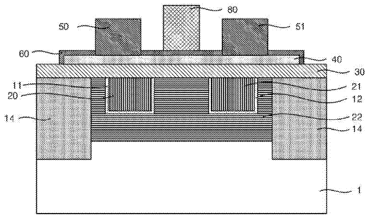
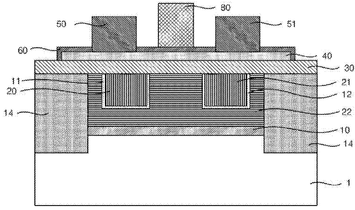
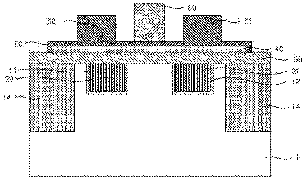
Reconfigurable electronic devices and operation method thereof
PatentActiveUS20160056301A1
Innovation
- The use of a reconfigurable electronic device structure with independently voltage-adjustable lower electrodes and a non-volatile memory function, incorporating 2D materials like graphene nanoribbons or TMDCs, and a bottom-up approach with single-walled carbon nanotubes, where lower electrodes are formed using deposition, etching, and CMP processes to improve position control and integration, and reduce parasitic components.

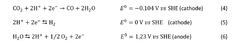
Use of semiconductors to control the selectivity of eletrochemical reduction of carbon dioxide
PatentWO2022153236A1
Innovation
- The use of semiconductor materials on the electrode side of electrolysers, either as electrocatalysts or in diode configurations, to control the energy level of electron delivery and mitigate proton recombination, thereby increasing faradaic efficiency and selectivity towards organic molecules and CO production.


Environmental Impact and Sustainability of 2D Catalytic Technologies
The environmental implications of catalytic reconfiguration technologies in 2D semiconductor systems extend far beyond their immediate applications. These technologies demonstrate significant potential for reducing the environmental footprint of electronic manufacturing processes, which traditionally involve energy-intensive fabrication methods and hazardous chemicals. By enabling precise atomic-level modifications at lower energy thresholds, 2D catalytic processes can substantially decrease energy consumption compared to conventional semiconductor manufacturing techniques.
Material efficiency represents another critical sustainability advantage. The atomically thin nature of 2D materials inherently requires less raw material input, while catalytic reconfiguration allows for targeted modifications without generating substantial waste. This approach aligns with circular economy principles by potentially extending device lifespans through in-situ reconfiguration rather than replacement, thereby reducing electronic waste that currently poses a significant environmental challenge globally.
Water conservation benefits emerge as 2D catalytic technologies typically require less intensive cleaning and processing steps compared to traditional semiconductor fabrication. This advantage becomes increasingly important as water scarcity affects more regions worldwide, particularly in areas with concentrated semiconductor manufacturing facilities.
The life cycle assessment of 2D catalytic technologies reveals promising sustainability metrics. Early studies indicate potential reductions in carbon footprint by 30-45% compared to conventional semiconductor processing when evaluated across the entire production chain. However, challenges remain in scaling these technologies while maintaining their environmental benefits, particularly regarding catalyst recovery and reuse.
Regulatory frameworks are evolving to address these emerging technologies. The European Union's REACH regulations and similar initiatives worldwide are beginning to incorporate provisions for nanomaterials and 2D systems, though specific guidelines for catalytic reconfiguration processes remain underdeveloped. Industry leaders are proactively establishing voluntary standards to demonstrate environmental stewardship while awaiting more comprehensive regulatory frameworks.
Future sustainability improvements may come through innovations in green catalysts derived from earth-abundant materials rather than rare or precious metals. Research into bio-inspired catalysts and environmentally benign reaction pathways shows particular promise for further reducing the ecological impact of these technologies while maintaining or enhancing their performance characteristics in semiconductor applications.
Scalability and Industrial Implementation Challenges
The scaling of catalytic reconfiguration technologies in 2D semiconductor systems from laboratory demonstrations to industrial-scale production presents significant challenges that must be addressed for commercial viability. Current fabrication methods for precise catalyst deposition on 2D materials often rely on expensive equipment and time-consuming processes that are difficult to scale. Electron beam lithography, commonly used for prototype development, offers nanometer precision but suffers from low throughput and high operational costs, making it impractical for mass production scenarios.
Material uniformity represents another critical barrier to industrial implementation. The performance of catalytic reconfiguration depends heavily on the quality and consistency of the 2D semiconductor substrate. While laboratory samples can be carefully selected for optimal properties, industrial-scale production requires consistent material quality across large areas. Current growth methods for 2D materials like transition metal dichalcogenides (TMDs) still struggle with defect control and thickness uniformity when scaled beyond a few centimeters.
Process integration with existing semiconductor manufacturing infrastructure presents both opportunities and obstacles. The semiconductor industry's established CMOS fabrication lines represent billions in capital investment that new technologies must leverage rather than replace. Adapting catalytic reconfiguration processes to be compatible with standard semiconductor equipment requires significant engineering effort to ensure process compatibility, yield management, and quality control across multiple fabrication steps.
Economic considerations further complicate industrial adoption. The cost-performance ratio of catalytically reconfigured 2D semiconductor devices must compete with established technologies. Current estimates suggest that material and processing costs need to decrease by at least an order of magnitude to achieve competitive pricing for consumer electronics applications. Additionally, the environmental impact of scaled production requires careful assessment, particularly regarding the use of rare metals as catalysts and potential waste streams from processing.
Reliability and device lifetime under real-world operating conditions remain largely unexplored at industrial scales. Laboratory demonstrations typically evaluate performance under controlled environments, whereas commercial devices must function reliably across wide temperature ranges, humidity levels, and mechanical stresses. Accelerated aging tests suggest potential degradation mechanisms in catalyst-semiconductor interfaces that could limit long-term stability, requiring further engineering solutions before mass deployment.
Standardization efforts are also lacking but essential for industrial implementation. The absence of agreed-upon testing protocols, performance metrics, and quality standards hampers supply chain development and slows industry adoption. Collaborative initiatives between academic institutions, industry consortia, and standards organizations will be necessary to establish the framework needed for commercial scaling of this promising technology.
Unlock deeper insights with PatSnap Eureka Quick Research — get a full tech report to explore trends and direct your research. Try now!
Generate Your Research Report Instantly with AI Agent
Supercharge your innovation with PatSnap Eureka AI Agent Platform!