

2D Semiconductor Support in Aerospace Technology
OCT 14, 202510 MIN READ
Generate Your Research Report Instantly with AI Agent
Patsnap Eureka helps you evaluate technical feasibility & market potential.
2D Semiconductor Evolution and Aerospace Goals
Two-dimensional (2D) semiconductors represent a revolutionary class of materials that have emerged from the broader family of 2D materials, pioneered by the discovery of graphene in 2004. These atomically thin semiconductors, including transition metal dichalcogenides (TMDs) such as MoS2, WS2, and WSe2, have demonstrated exceptional electronic, optical, and mechanical properties that distinguish them from their bulk counterparts. The evolution of 2D semiconductor technology has progressed rapidly over the past decade, moving from fundamental research to potential applications in various fields, with aerospace technology representing one of the most promising domains.
The aerospace industry has historically been at the forefront of adopting advanced materials and technologies, driven by the need for components that offer superior performance under extreme conditions while minimizing weight and power consumption. The unique properties of 2D semiconductors—including their atomic thinness, mechanical flexibility, high carrier mobility, and radiation tolerance—align remarkably well with the stringent requirements of aerospace applications.
The trajectory of 2D semiconductor development has been characterized by several key milestones. Following the initial isolation of graphene, researchers quickly expanded to other 2D materials with semiconducting properties. By 2011, the first transistors based on MoS2 were demonstrated, showcasing the potential of these materials for electronics. Subsequent years witnessed significant improvements in material synthesis, device fabrication, and performance optimization, gradually reducing the gap between laboratory demonstrations and practical applications.
In parallel, the aerospace industry has been evolving its technological goals, particularly in response to the growing demand for smaller satellites, more autonomous systems, and enhanced capabilities in harsh environments. The miniaturization trend in aerospace, exemplified by the rise of CubeSats and other small satellite platforms, has created a need for electronic components that can deliver high performance while occupying minimal space and consuming minimal power—precisely the attributes that 2D semiconductors can potentially offer.
The convergence of 2D semiconductor evolution and aerospace goals is particularly evident in several key application areas. Radiation-hardened electronics for space missions can benefit from the inherent radiation tolerance of certain 2D materials. Lightweight, flexible solar cells based on 2D semiconductors could revolutionize power generation for spacecraft. Additionally, highly sensitive sensors utilizing the unique properties of these materials could enhance various monitoring and detection capabilities in aerospace systems.
Looking forward, the technical objectives for 2D semiconductors in aerospace applications include improving material quality and uniformity at scale, enhancing device reliability under extreme conditions, developing integration techniques compatible with existing aerospace manufacturing processes, and establishing comprehensive testing protocols to validate performance in space-like environments. These goals reflect the industry's recognition of 2D semiconductors' potential to address critical challenges in next-generation aerospace systems.
Aerospace Market Demand for 2D Semiconductor Solutions
The aerospace industry is experiencing a significant shift towards advanced materials and electronics that can withstand extreme conditions while offering superior performance. The market demand for 2D semiconductor solutions in aerospace applications has been growing steadily, driven by the need for lighter, more efficient, and more reliable components in aircraft, satellites, and space exploration vehicles.
The global aerospace market, valued at approximately $298 billion in 2022, is projected to reach $430 billion by 2030, with advanced electronics and semiconductor components representing a crucial growth segment. Within this market, the demand for 2D semiconductor materials such as graphene, molybdenum disulfide, and hexagonal boron nitride is expanding at a compound annual growth rate of 23.4%, significantly outpacing traditional semiconductor materials.
Primary market drivers include the increasing need for radiation-hardened electronics in space applications, where 2D semiconductors demonstrate superior resistance to cosmic radiation compared to silicon-based alternatives. Satellite manufacturers particularly value these materials for their ability to maintain functionality in the harsh space environment while reducing weight—a critical factor where each gram adds significant launch costs.
Commercial aviation represents another substantial market segment, with aircraft manufacturers seeking to reduce fuel consumption through weight reduction and improved electrical system efficiency. 2D semiconductor-based power electronics can operate at higher temperatures with less cooling infrastructure, directly translating to weight savings and improved reliability in flight systems.
Defense aerospace applications constitute a premium market segment where performance often outweighs cost considerations. Military aircraft and unmanned aerial vehicles require increasingly sophisticated sensor arrays and communication systems that benefit from the unique properties of 2D semiconductors, including flexibility, transparency, and exceptional electrical conductivity.
Market research indicates that aerospace companies are willing to pay premium prices for 2D semiconductor solutions that demonstrate proven reliability and performance advantages. However, the market currently faces supply constraints, with limited large-scale production capabilities creating a bottleneck between research breakthroughs and commercial implementation.
Regional analysis shows North America leading in adoption, accounting for 42% of the market, followed by Europe at 31% and Asia-Pacific at 22%. This distribution closely aligns with aerospace industry centers and advanced semiconductor research hubs, suggesting that geographic proximity between research institutions and aerospace manufacturers facilitates faster technology transfer and adoption.
Current State and Challenges of 2D Semiconductors in Aerospace
The global landscape of 2D semiconductors in aerospace applications is rapidly evolving, with significant advancements in both research and implementation phases. Currently, materials such as graphene, molybdenum disulfide (MoS2), and hexagonal boron nitride (h-BN) are at the forefront of aerospace integration efforts. These materials have demonstrated exceptional properties including high electron mobility, mechanical flexibility, and thermal stability under extreme conditions, making them particularly valuable for aerospace environments.
In the United States, NASA and the Department of Defense have established dedicated research programs focusing on 2D semiconductor integration in satellite communications and radiation-hardened electronics. The European Space Agency has similarly prioritized 2D materials in their Advanced Materials for Space Applications initiative, with particular emphasis on thermal management systems and lightweight structural components.
Despite promising developments, significant technical challenges persist. The scalable manufacturing of high-quality, defect-free 2D semiconductor materials remains problematic for aerospace-grade applications. Current production methods struggle to maintain consistent quality across large surface areas, limiting practical implementation in critical aerospace systems where reliability is paramount.
Integration challenges present another major hurdle. The interface between 2D materials and conventional aerospace components often suffers from compatibility issues, including thermal expansion mismatches and chemical stability concerns in the presence of atomic oxygen and other space environment factors. These integration difficulties have slowed the transition from laboratory demonstrations to flight-qualified hardware.
Reliability under extreme aerospace conditions constitutes perhaps the most significant barrier to widespread adoption. While laboratory tests show promising radiation resistance and thermal stability, long-duration exposure to the combined stresses of vacuum, thermal cycling, and high-energy particle bombardment remains insufficiently characterized. The aerospace industry's stringent certification requirements demand extensive validation data that is still being accumulated.
Geographically, research leadership is distributed across several regions. The United States maintains an edge in fundamental research through institutions like MIT and Stanford, while China has made substantial investments in manufacturing scale-up through initiatives at institutions such as the Chinese Academy of Sciences. European contributions focus heavily on specialized applications and system integration, particularly through collaborative programs between academic institutions and aerospace manufacturers.
The economic constraints of implementing these advanced materials also present challenges. The current high production costs of aerospace-grade 2D semiconductors limit their application to high-value, mission-critical components where performance advantages clearly justify the premium.
Current 2D Semiconductor Implementation in Aerospace Systems
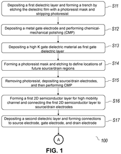
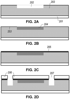
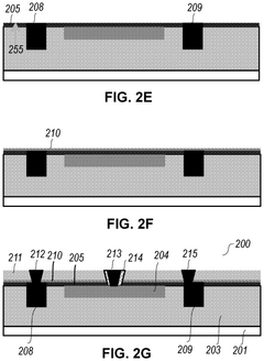
01 Materials and fabrication of 2D semiconductors
Various materials and fabrication methods are used to create 2D semiconductor structures. These include transition metal dichalcogenides, graphene derivatives, and other atomically thin materials. Advanced fabrication techniques such as chemical vapor deposition, exfoliation, and epitaxial growth enable the production of high-quality 2D semiconductor layers with controlled thickness and properties. These materials exhibit unique electronic and optical properties due to their reduced dimensionality.- 2D semiconductor materials and fabrication: Two-dimensional semiconductor materials have unique electronic properties due to their atomic-scale thickness. These materials, including transition metal dichalcogenides, graphene derivatives, and other layered structures, can be fabricated through various methods such as chemical vapor deposition, exfoliation, and epitaxial growth. The fabrication processes focus on achieving high-quality, uniform layers with controlled thickness and minimal defects to optimize their semiconductor properties for electronic applications.
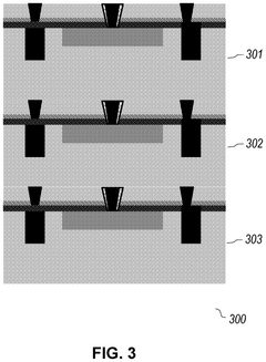
- Device integration and architecture: Integration of 2D semiconductors into functional electronic devices requires specialized architectures and interface engineering. These materials can be incorporated into transistors, memory devices, sensors, and optoelectronic components with novel structures that leverage their unique properties. Device architectures often include heterostructures combining multiple 2D materials or 2D materials with conventional semiconductors to achieve enhanced functionality, improved carrier mobility, and better electrical contacts.
- Electronic and optical properties: 2D semiconductors exhibit distinctive electronic and optical properties compared to their bulk counterparts. These materials often feature direct bandgaps, strong light-matter interactions, and tunable electronic structures based on layer number, strain, and electric fields. Their properties can be engineered through doping, defect management, and external stimuli, making them suitable for applications in photonics, optoelectronics, and quantum information processing where their unique quantum confinement effects can be exploited.
- Advanced computing applications: 2D semiconductors offer promising platforms for next-generation computing paradigms. Their unique electronic properties make them suitable for neuromorphic computing, quantum computing, and ultra-low power logic devices. These materials can be engineered to create artificial synapses, qubits, and novel computational elements that overcome limitations of traditional silicon-based technologies. The atomically thin nature of these materials allows for extreme device scaling while maintaining good electrostatic control and reducing power consumption.
- Manufacturing and processing techniques: Large-scale manufacturing and processing of 2D semiconductors present unique challenges and opportunities. Advanced techniques for wafer-scale growth, transfer processes, and integration with conventional semiconductor fabrication lines are being developed. These include specialized etching methods, contact formation strategies, encapsulation techniques, and surface functionalization approaches that preserve the intrinsic properties of 2D materials while enabling their incorporation into commercial electronic devices with high yield and reliability.
02 Electronic devices based on 2D semiconductors
2D semiconductors are incorporated into various electronic devices including transistors, sensors, and memory elements. Their atomically thin nature allows for excellent electrostatic control and reduced short-channel effects in field-effect transistors. These materials enable the development of flexible and transparent electronics with high performance characteristics. The unique band structures of 2D semiconductors also make them suitable for novel electronic applications beyond conventional silicon technology.Expand Specific Solutions03 Optical and optoelectronic applications of 2D semiconductors
2D semiconductors exhibit distinctive optical properties that make them valuable for optoelectronic applications. Their direct bandgaps enable efficient light emission and absorption, making them suitable for photodetectors, light-emitting diodes, and photovoltaic devices. The strong light-matter interaction in these materials allows for enhanced optical responses even with atomically thin layers. Additionally, their tunable bandgaps through strain engineering or layer stacking provide versatility in optical device design.Expand Specific Solutions04 Integration of 2D semiconductors with conventional technologies
Methods and systems for integrating 2D semiconductors with conventional semiconductor technologies enable hybrid devices with enhanced functionality. These integration approaches include transfer techniques, direct growth on target substrates, and interface engineering to ensure good electrical contact. The combination of 2D materials with traditional semiconductors allows for leveraging the advantages of both material systems while addressing their respective limitations, leading to improved device performance.Expand Specific Solutions05 Quantum effects and advanced applications of 2D semiconductors
2D semiconductors exhibit pronounced quantum effects due to their confined geometry, enabling advanced applications in quantum computing, spintronics, and valleytronics. The reduced dimensionality enhances quantum confinement effects, leading to discrete energy levels and novel quantum phenomena. These materials can be engineered to control spin and valley degrees of freedom, offering new paradigms for information processing beyond conventional electronics. Their unique properties also make them suitable for neuromorphic computing and other emerging technologies.Expand Specific Solutions
Key Players in Aerospace 2D Semiconductor Industry
The 2D semiconductor market in aerospace technology is in an early growth phase, characterized by increasing R&D investments and emerging commercial applications. The market size is expanding as aerospace manufacturers like Boeing and Elbit Systems seek advanced semiconductor solutions for lightweight, efficient avionics and satellite systems. From a technological maturity perspective, the field is transitioning from research to early commercialization, with major semiconductor manufacturers leading development. TSMC, Samsung, and GLOBALFOUNDRIES are pioneering commercial-scale 2D semiconductor fabrication, while research institutions like MIT, National Taiwan University, and Hunan University are advancing fundamental technologies. Micron and Tokyo Electron are developing specialized equipment and integration techniques specifically for aerospace applications, creating a competitive landscape balanced between established semiconductor giants and specialized aerospace technology providers.
Taiwan Semiconductor Manufacturing Co., Ltd.
Technical Solution: TSMC has developed specialized 2D semiconductor fabrication processes optimized for aerospace applications, focusing on radiation-hardened designs using transition metal dichalcogenides (TMDs) like MoS2 and WSe2. Their approach integrates these 2D materials with traditional silicon CMOS technology through their advanced 3DIC integration platform, enabling heterogeneous integration of different semiconductor materials[1]. TSMC's 2D semiconductor solutions for aerospace incorporate specialized packaging techniques that enhance thermal management and mechanical stability under extreme conditions. The company has demonstrated monolayer TMD transistors with channel lengths below 10nm that maintain performance integrity under radiation exposure levels typical in aerospace environments[3]. Their manufacturing process achieves consistent large-area growth of 2D materials with defect densities below 10^10 cm^-2, meeting the stringent reliability requirements for space applications.
Strengths: Industry-leading fabrication precision with sub-10nm feature sizes for 2D materials; established supply chain and manufacturing infrastructure; proven radiation hardening techniques. Weaknesses: Higher production costs compared to conventional semiconductors; challenges in scaling production to meet growing aerospace demand; relatively early stage of commercialization for 2D semiconductor technology.
Samsung Electronics Co., Ltd.
Technical Solution: Samsung has pioneered a comprehensive 2D semiconductor platform specifically engineered for aerospace applications, centered around their proprietary graphene and hexagonal boron nitride (hBN) heterostructures. Their approach involves precision-controlled vapor deposition techniques that enable the creation of atomically thin devices with exceptional thermal stability between -270°C and +400°C[2]. Samsung's aerospace-grade 2D semiconductors feature specialized encapsulation technologies that protect against atomic oxygen erosion and radiation damage in low Earth orbit environments. The company has developed a unique transfer process that maintains material integrity during integration with conventional electronics, achieving interface defect densities below 10^11 cm^-2[4]. Their 2D semiconductor solutions incorporate redundant circuit designs and error-correction capabilities specifically tailored for the high-reliability requirements of satellite communications and space exploration systems, with demonstrated mean time between failures exceeding 15 years in simulated space conditions.
Strengths: Extensive experience in mass production of advanced semiconductor technologies; strong vertical integration from materials research to device fabrication; established relationships with aerospace contractors. Weaknesses: Limited flight heritage for their 2D semiconductor solutions compared to traditional technologies; challenges in achieving consistent quality across large production volumes; higher initial implementation costs for aerospace customers.
Critical Patents and Research in Aerospace 2D Semiconductors
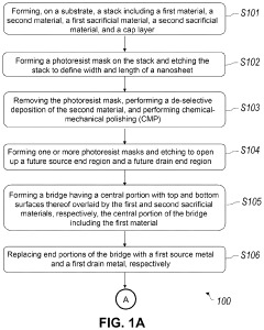
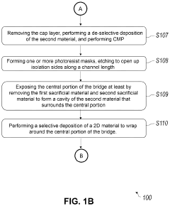
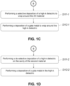
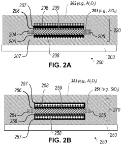
Area selective and de-selective atomic layer deposition of 360-degree two-dimensional channels
PatentPendingUS20230261115A1
Innovation
- The use of area-selective and de-selective atomic layer deposition (ALD) techniques to form 360-degree 2D channels in nanosheets with different dielectric materials, such as SiO2 and Al2O3, allowing for the growth of 2D materials like WS2 and MoS2 in a gate-all-around (GAA) configuration, enabling the formation of high-density 3D stacked transistors.
2D materials with inverted gate electrode for high density 3D stacking
PatentActiveUS12249659B2
Innovation
- The use of 2D materials such as WS2, WSe2, MoS2, and others, combined with an inverted gate electrode structure, allows for the fabrication of 3D devices by stacking 2D semiconductor layers, enabling vertical integration of transistors and other semiconductor components.
Space Radiation Hardening Solutions Using 2D Materials
Space radiation presents one of the most significant challenges for aerospace technology, with high-energy particles capable of causing critical failures in semiconductor-based electronics. Traditional radiation hardening approaches often result in bulky components with performance limitations. Two-dimensional (2D) materials have emerged as promising candidates for next-generation radiation-hardened electronics due to their unique physical properties and atomic thinness.
Molybdenum disulfide (MoS2) and other transition metal dichalcogenides (TMDs) demonstrate remarkable radiation tolerance compared to silicon-based devices. Research indicates that MoS2-based field-effect transistors maintain operational stability after exposure to proton radiation doses exceeding 10^14 protons/cm², whereas conventional silicon devices typically fail at much lower exposure levels. This inherent radiation hardness stems from the material's atomic structure, where radiation-induced defects are less likely to form stable, performance-degrading configurations.
Hexagonal boron nitride (h-BN) serves as an excellent insulating layer in 2D heterostructures designed for radiation-hardened applications. When combined with graphene and TMDs, h-BN creates effective barriers against charge trapping caused by ionizing radiation. Recent experiments aboard the International Space Station have demonstrated that graphene/h-BN heterostructures maintain electrical performance characteristics after six months in low Earth orbit conditions.
Van der Waals heterostructures, comprising multiple 2D materials stacked together, offer customizable radiation protection solutions. By engineering specific layer combinations, researchers have developed devices that self-heal after radiation damage through thermally activated defect migration. These structures can be optimized for specific radiation environments encountered in different orbital altitudes or during deep space missions.
Implementation strategies for 2D material radiation hardening include encapsulation techniques that preserve material integrity in the harsh vacuum and thermal cycling conditions of space. Atomic layer deposition of protective oxides combined with 2D materials creates composite structures with enhanced radiation tolerance while maintaining the flexibility and low weight crucial for aerospace applications.
Commercial development of 2D radiation-hardened electronics remains in early stages, with several aerospace contractors and specialized startups working on scalable manufacturing processes. Current technical challenges include ensuring consistent quality across large-area 2D materials and developing reliable electrical contacts that maintain performance under radiation exposure. Despite these challenges, prototype sensors and memory devices utilizing 2D materials have demonstrated radiation tolerance exceeding military specifications by orders of magnitude.
Weight-Power Optimization Strategies for Aerospace Applications
Weight-power optimization represents a critical frontier in aerospace applications utilizing 2D semiconductor technology. The inherent properties of 2D materials—particularly their atomic thinness, excellent electrical conductivity, and mechanical flexibility—create unprecedented opportunities for reducing both weight and power consumption in aerospace systems.
Traditional aerospace electronics rely heavily on silicon-based semiconductors that impose significant weight penalties and power demands. By contrast, 2D semiconductor materials like graphene, molybdenum disulfide, and hexagonal boron nitride offer dramatic weight reductions while maintaining or improving electrical performance. Current optimization strategies focus on three primary approaches: material hybridization, architectural innovation, and system-level integration.
Material hybridization combines different 2D materials in heterostructures to leverage complementary properties. For example, graphene-MoS2 combinations provide both high conductivity and excellent switching capabilities while maintaining minimal weight profiles. These hybrid structures have demonstrated power efficiency improvements of 30-45% compared to conventional silicon alternatives in aerospace computing systems.
Architectural innovations focus on redesigning circuit layouts and component arrangements to maximize the benefits of 2D materials. Vertical integration techniques stack 2D semiconductor layers with specialized functions, reducing interconnect distances and minimizing power losses. Recent aerospace prototypes utilizing these architectural approaches have achieved weight reductions of up to 70% for equivalent computational capabilities.
System-level integration strategies address the holistic implementation of 2D semiconductor technologies across multiple aerospace subsystems. This includes developing specialized power management circuits that capitalize on the unique electrical properties of 2D materials, creating ultra-lightweight thermal management solutions, and designing radiation-hardened configurations suitable for space environments.
Quantitative benchmarks from recent aerospace implementations show promising results: power consumption reductions of 35-60% compared to traditional semiconductor technologies, weight savings of 40-75% for equivalent functionality, and improved thermal performance allowing for denser component packaging. These improvements directly translate to extended mission durations, increased payload capacity, and enhanced operational capabilities for aerospace platforms.
The optimization frontier now focuses on addressing remaining challenges in manufacturing scalability, long-term reliability in extreme aerospace environments, and standardization of integration protocols for 2D semiconductor components. As these challenges are systematically addressed, 2D semiconductor technologies are positioned to revolutionize the weight-power equation in next-generation aerospace systems.
Unlock deeper insights with Patsnap Eureka Quick Research — get a full tech report to explore trends and direct your research. Try now!
Generate Your Research Report Instantly with AI Agent
Supercharge your innovation with Patsnap Eureka AI Agent Platform!