Why 2D Semiconductors Are Critical in New Tech
OCT 14, 20259 MIN READ
Generate Your Research Report Instantly with AI Agent
Patsnap Eureka helps you evaluate technical feasibility & market potential.
2D Semiconductor Evolution and Research Objectives
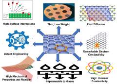
Two-dimensional (2D) semiconductors represent a revolutionary class of materials that have emerged from the discovery of graphene in 2004. Unlike traditional three-dimensional bulk semiconductors, these atomically thin materials exhibit unique electronic, optical, and mechanical properties that arise from quantum confinement effects when electrons are restricted to movement in a plane. The evolution of 2D semiconductor research has progressed from initial fundamental studies to increasingly sophisticated applications across multiple technology domains.
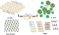
The journey began with graphene, a single layer of carbon atoms arranged in a hexagonal lattice. Despite its remarkable properties including exceptional electrical conductivity and mechanical strength, graphene's lack of a natural bandgap limited its semiconductor applications. This limitation catalyzed exploration of other 2D materials, particularly transition metal dichalcogenides (TMDs) such as MoS2, WS2, and WSe2, which possess natural bandgaps suitable for semiconductor applications.
By the mid-2010s, research expanded to include other 2D material families including hexagonal boron nitride (h-BN), black phosphorus, and MXenes. The field further evolved with the development of van der Waals heterostructures—artificial materials created by stacking different 2D materials to engineer specific properties and functionalities. This approach has enabled unprecedented control over electronic and optical characteristics at the atomic scale.
Recent advancements have focused on addressing key challenges including large-scale synthesis, precise control of layer numbers, defect management, and contact engineering. Significant progress has been made in chemical vapor deposition (CVD) techniques, allowing for wafer-scale production of high-quality 2D semiconductor films—a critical step toward industrial viability.
The primary research objectives in this field now center on several key areas. First, developing scalable and reproducible fabrication methods that maintain material quality while enabling integration with existing semiconductor manufacturing processes. Second, engineering stable and efficient electrical contacts to fully leverage the intrinsic properties of 2D materials. Third, exploring novel device architectures that exploit the unique characteristics of these materials, particularly for applications where conventional semiconductors face fundamental limitations.
Additional research priorities include understanding and controlling the interface physics between 2D materials and their surroundings, developing effective doping strategies, and enhancing material stability under operational conditions. The ultimate goal is to establish 2D semiconductors as a complementary technology to silicon, particularly for next-generation electronics, optoelectronics, quantum computing, and flexible/wearable devices where their exceptional properties offer distinct advantages over traditional semiconductor materials.
Market Applications and Growth Potential
The 2D semiconductor market is experiencing rapid growth, with projections indicating a compound annual growth rate of 19.6% from 2023 to 2030, potentially reaching a market value of $5.7 billion by 2030. This remarkable expansion is driven by the unique properties of 2D materials that enable applications impossible with traditional 3D semiconductors. The market demand spans across multiple high-growth sectors, creating diverse revenue streams for manufacturers and developers.
In the electronics sector, 2D semiconductors are revolutionizing transistor design, enabling the development of ultra-thin, flexible, and energy-efficient devices. Major smartphone manufacturers are investing heavily in 2D material research to create next-generation displays and processors that consume significantly less power while delivering enhanced performance. The wearable technology market, valued at over $61 billion in 2022, represents another substantial growth opportunity for 2D semiconductors, particularly in health monitoring devices requiring flexible, lightweight components.
The renewable energy sector presents perhaps the most promising growth avenue for 2D materials. Molybdenum disulfide and other transition metal dichalcogenides have demonstrated exceptional photovoltaic properties, potentially increasing solar cell efficiency by up to 27% compared to current silicon-based technologies. This application alone could drive market growth as global solar capacity installations continue to accelerate, with annual additions exceeding 200 GW in recent years.
Healthcare applications represent an emerging but rapidly expanding market segment. 2D materials' biocompatibility and unique electrical properties make them ideal for biosensors and diagnostic devices. The global biosensor market, growing at 8.2% annually, offers substantial opportunities for 2D semiconductor integration, particularly in point-of-care testing devices and continuous health monitoring systems.
Automotive and aerospace industries are increasingly adopting 2D semiconductors for lightweight, high-performance components. The electric vehicle market, growing at over 21% annually, requires advanced battery management systems and power electronics where 2D materials excel. Similarly, aerospace applications benefit from the weight reduction and performance improvements offered by these materials.
Regional market analysis reveals Asia-Pacific as the dominant manufacturing hub, with China, South Korea, and Japan leading production capacity development. North America maintains leadership in research and development, while Europe focuses on specialized applications in automotive and industrial sectors. This geographic distribution creates a complex but robust global supply chain, though recent geopolitical tensions have highlighted vulnerabilities that may impact future growth trajectories.
Global Development Status and Technical Barriers
The global landscape of 2D semiconductor development has witnessed remarkable progress over the past decade, with research centers across North America, Europe, and Asia making significant contributions. The United States maintains leadership through institutions like MIT, Stanford, and national laboratories, focusing on fundamental research and novel applications. European research clusters, particularly in the UK, Germany, and Switzerland, have established strong positions in materials characterization and quantum applications of 2D semiconductors.
Asia has emerged as a formidable competitor, with China investing heavily in 2D materials research infrastructure and South Korea leveraging its semiconductor manufacturing expertise to advance 2D technology integration. Japan continues to excel in precision fabrication techniques, while Singapore has positioned itself as a hub for 2D semiconductor commercialization in Southeast Asia.
Despite this global progress, several critical technical barriers impede the widespread adoption of 2D semiconductors. The most significant challenge remains scalable manufacturing, as current laboratory-scale production methods like mechanical exfoliation cannot meet industrial demands. Chemical vapor deposition shows promise but struggles with uniformity and defect control across large areas.
Contact engineering presents another substantial hurdle, as the atomically thin nature of 2D semiconductors creates unique challenges in forming low-resistance electrical contacts without damaging the material's intrinsic properties. The interface between 2D materials and conventional 3D materials often introduces performance-limiting defects and resistance.
Encapsulation and environmental stability represent persistent challenges, as many 2D semiconductors exhibit sensitivity to oxygen, moisture, and other environmental factors that can rapidly degrade their electronic properties. Developing effective passivation techniques without compromising device performance remains an active research area.
Integration with existing silicon-based technologies presents compatibility issues, as the processing conditions for 2D materials often conflict with established CMOS fabrication protocols. Temperature constraints, chemical compatibility, and mechanical handling differences require significant process modifications.
Material quality and consistency also remain problematic, with variations in layer thickness, defect density, and grain boundaries significantly affecting device performance. The lack of standardized characterization methods further complicates quality control across different research and manufacturing facilities.
Addressing these technical barriers requires coordinated international efforts combining fundamental research with applied engineering approaches. Recent collaborative initiatives between academic institutions and industry partners show promising directions toward overcoming these challenges, potentially accelerating the timeline for commercial viability of 2D semiconductor technologies.
Current 2D Semiconductor Implementation Approaches
01 Materials and fabrication of 2D semiconductors
Various materials and fabrication methods are used to create 2D semiconductor structures. These include transition metal dichalcogenides, graphene derivatives, and other atomically thin materials. Advanced fabrication techniques such as chemical vapor deposition, mechanical exfoliation, and epitaxial growth enable the production of high-quality 2D semiconductor layers with controlled thickness and properties. These materials exhibit unique electronic and optical properties due to their reduced dimensionality.- Materials and fabrication of 2D semiconductors: Two-dimensional semiconductor materials are fabricated using various techniques to create atomically thin layers with unique electronic properties. These materials include transition metal dichalcogenides, graphene derivatives, and other layered structures. The fabrication methods involve exfoliation, chemical vapor deposition, and epitaxial growth to achieve high-quality 2D semiconductor layers suitable for electronic applications.
- Electronic devices based on 2D semiconductors: Two-dimensional semiconductors are integrated into various electronic devices including transistors, sensors, and memory elements. These materials offer advantages such as flexibility, transparency, and unique quantum properties that enable novel device architectures. The atomically thin nature of 2D semiconductors allows for efficient carrier transport and electrostatic control, making them promising candidates for next-generation electronics.
- Optoelectronic applications of 2D semiconductors: Two-dimensional semiconductors exhibit exceptional optical properties that make them suitable for various optoelectronic applications. These materials feature direct bandgaps, strong light-matter interactions, and tunable optical responses. They are utilized in photodetectors, light-emitting devices, photovoltaics, and optical modulators, offering advantages in terms of efficiency, flexibility, and integration with conventional electronics.
- Heterostructures and interfaces in 2D semiconductors: Heterostructures formed by stacking different 2D semiconductor materials create unique interfaces with novel electronic and optical properties. These van der Waals heterostructures enable band alignment engineering, interlayer excitons, and quantum confinement effects. The atomically sharp interfaces between different 2D materials allow for precise control of carrier dynamics and energy transfer, opening possibilities for quantum devices and advanced electronics.
- Processing and integration technologies for 2D semiconductors: Various processing and integration technologies have been developed to incorporate 2D semiconductors into practical devices and systems. These include transfer techniques, contact engineering, doping methods, and encapsulation strategies to preserve the intrinsic properties of 2D materials. Advanced lithography, etching, and packaging approaches enable the integration of 2D semiconductors with conventional electronics and other functional materials for practical applications.
02 Electronic devices based on 2D semiconductors
2D semiconductors are incorporated into various electronic devices including transistors, memory cells, sensors, and integrated circuits. The atomically thin nature of these materials allows for the creation of ultra-compact devices with improved performance characteristics. These devices often demonstrate superior electron mobility, flexibility, and power efficiency compared to conventional semiconductor technologies, making them promising candidates for next-generation electronics.Expand Specific Solutions03 Optical and optoelectronic applications of 2D semiconductors
2D semiconductors exhibit unique optical properties that make them suitable for various optoelectronic applications. These materials can be used in photodetectors, light-emitting devices, photovoltaic cells, and optical modulators. Their direct bandgap nature, strong light-matter interaction, and tunable optical properties enable the development of highly efficient and compact optoelectronic devices with enhanced performance characteristics.Expand Specific Solutions04 Integration of 2D semiconductors with other materials
The integration of 2D semiconductors with other materials creates heterostructures with enhanced functionality. These include vertical stacking of different 2D materials, combination with conventional semiconductors, and incorporation into flexible substrates. Such hybrid structures enable new device architectures and functionalities by leveraging the complementary properties of different materials, resulting in improved performance and novel applications in electronics and optoelectronics.Expand Specific Solutions05 Computational methods for 2D semiconductor design
Computational methods play a crucial role in the design and analysis of 2D semiconductor materials and devices. These include simulation techniques, machine learning approaches, and quantum mechanical calculations to predict and optimize material properties and device performance. Advanced modeling enables the exploration of novel 2D semiconductor structures and their behavior under various conditions, accelerating the development of new materials and applications.Expand Specific Solutions
Leading Companies and Research Institutions
The 2D semiconductor market is in a growth phase, characterized by increasing investments and research activities. The market is projected to expand significantly due to applications in next-generation electronics, with an estimated compound annual growth rate of 15-20%. Technologically, 2D semiconductors are transitioning from research to early commercialization, with major players like Taiwan Semiconductor Manufacturing Co., Samsung Electronics, and GlobalFoundries leading industrial development. Academic institutions such as MIT, Tsinghua University, and National Taiwan University are driving fundamental research, while companies like Huawei and IMEC are focusing on application development. The collaboration between industry and academia is accelerating the maturation of 2D semiconductor technology for future electronic devices.
Taiwan Semiconductor Manufacturing Co., Ltd.
Technical Solution: TSMC has pioneered advanced manufacturing processes for 2D semiconductors, particularly focusing on transition metal dichalcogenides (TMDs) like MoS2 and WSe2. Their approach involves atomic layer deposition techniques that enable precise control over 2D material growth at industrial scale. TSMC has developed specialized etching and transfer processes that maintain the integrity of atomically thin materials during integration with conventional CMOS technology. Their 2D semiconductor fabrication platform incorporates specialized contact engineering to overcome the high contact resistance typically associated with 2D materials, achieving resistance values below 200 Ω·μm. TSMC has also made significant progress in developing gate dielectrics specifically optimized for 2D semiconductor interfaces, reducing interface trap densities by an order of magnitude compared to conventional approaches.
Strengths: Industry-leading manufacturing infrastructure, exceptional process control capabilities, and established supply chain integration. Weaknesses: Higher production costs compared to conventional semiconductors and challenges in scaling production to meet potential future demand for 2D semiconductor devices.
Samsung Electronics Co., Ltd.
Technical Solution: Samsung has developed a comprehensive 2D semiconductor technology platform centered around graphene and transition metal dichalcogenides (TMDs). Their approach focuses on large-area synthesis methods using metal-organic chemical vapor deposition (MOCVD) that achieves monolayer uniformity exceeding 95% across 300mm wafers. Samsung's integration strategy employs a unique "2D-first" process flow where 2D materials are synthesized early in the manufacturing sequence and protected during subsequent high-temperature steps. They've pioneered specialized doping techniques for 2D semiconductors using plasma-assisted processes that achieve carrier concentrations up to 10^13 cm^-2 while maintaining mobility. Samsung has also developed novel heterostructure architectures combining different 2D materials (such as MoS2/WSe2) to create atomically sharp p-n junctions with switching ratios exceeding 10^8.
Strengths: Vertical integration from materials research to device fabrication, strong intellectual property portfolio in 2D materials, and ability to leverage existing semiconductor manufacturing infrastructure. Weaknesses: Relatively high defect densities in synthesized 2D materials and challenges in achieving consistent electrical performance across large wafer areas.
Breakthrough Patents and Scientific Publications
2d materials and their electronic and physical properties in transistors
PatentPendingIN202211063311A
Innovation
- The development of a sensor arrangement using a field-effect transistor with an atomically thin channel structure, specifically leveraging two-dimensional materials such as graphene and molybdenum disulfide, which exhibit sensitive electrical reactions and low noise levels, enabling ultrasensitive detection of biomolecules by forming heterojunctions and utilizing advanced nanoscale fabrication methods like PLD and high dynamic energy impingement to create sensitive biosensors.
Material Supply Chain Analysis
The global supply chain for 2D semiconductor materials represents a complex network of extraction, processing, and distribution channels that are critical to the advancement of next-generation technologies. Currently, the supply chain is heavily concentrated in specific geographical regions, with China dominating the production of graphene and transition metal dichalcogenides (TMDs), while South Korea and Japan lead in high-quality substrate materials essential for 2D semiconductor fabrication.
Raw material extraction presents significant challenges, particularly for rare earth elements used in certain 2D semiconductor compositions. The limited number of economically viable mining operations creates potential bottlenecks in the supply chain, with over 70% of rare earth processing occurring in China. This concentration introduces geopolitical vulnerabilities that technology companies must navigate when securing consistent material supplies.
Processing capabilities for 2D materials require specialized equipment and expertise, creating another potential constraint in the supply chain. The high-precision manufacturing processes needed for atomically thin materials demand ultra-clean environments and advanced lithography systems, which are primarily produced by a small number of companies in the Netherlands, Japan, and the United States.
Sustainability concerns are increasingly influencing supply chain decisions for 2D semiconductor materials. The extraction of certain elements used in these materials can have significant environmental impacts, prompting research into more environmentally friendly synthesis methods and recycling processes. Companies investing in 2D semiconductor technologies are increasingly implementing responsible sourcing practices to mitigate these concerns.
Vertical integration strategies are emerging among leading technology companies seeking to secure their supply chains. Companies like Samsung and Intel have begun investing in direct relationships with material suppliers or developing in-house production capabilities for critical 2D materials, reducing dependency on external suppliers and mitigating supply chain risks.
The COVID-19 pandemic exposed vulnerabilities in the global semiconductor supply chain, prompting governments worldwide to invest in domestic production capabilities. The CHIPS Act in the United States and similar initiatives in Europe and Asia aim to diversify the geographical distribution of semiconductor manufacturing, including advanced materials like 2D semiconductors, potentially reshaping the supply chain landscape over the next decade.
Environmental Impact and Sustainability Factors
The environmental footprint of 2D semiconductors represents a significant advantage over traditional silicon-based technologies. These atomically thin materials require substantially less raw material for production, potentially reducing mining impacts and resource depletion associated with conventional semiconductor manufacturing. For instance, transition metal dichalcogenides (TMDs) like MoS2 and WSe2 can function effectively with just a few atomic layers, compared to the bulk materials needed in traditional semiconductor fabrication.
Manufacturing processes for 2D semiconductors also demonstrate promising sustainability characteristics. Lower processing temperatures are typically required for 2D material production compared to silicon, which traditionally demands energy-intensive high-temperature processes. This temperature reduction translates directly to decreased energy consumption and associated carbon emissions during manufacturing phases.
The operational efficiency of 2D semiconductor devices further enhances their environmental profile. Their unique electronic properties enable lower power consumption in end applications, extending battery life in portable devices and reducing overall energy demands in larger systems. This efficiency becomes particularly critical as computing demands continue to escalate globally, offering a pathway to mitigate the growing energy footprint of the technology sector.
End-of-life considerations also favor 2D semiconductors. Their minimal material usage potentially simplifies recycling processes, while some research indicates possibilities for biodegradable or environmentally benign 2D materials that could reduce electronic waste concerns. This aspect becomes increasingly important as electronic waste continues to represent one of the fastest-growing waste streams globally.
Water usage represents another critical environmental factor where 2D semiconductors may offer advantages. Traditional semiconductor fabrication is notoriously water-intensive, while emerging production methods for 2D materials show potential for reduced water requirements, particularly important in regions facing water scarcity challenges.
Despite these advantages, challenges remain in scaling production methods for 2D semiconductors to industrial levels while maintaining their environmental benefits. Current laboratory-scale production methods may utilize hazardous chemicals or energy-intensive processes that would need optimization for truly sustainable large-scale manufacturing. Comprehensive lifecycle assessments are still needed to fully quantify the comparative environmental impacts across different semiconductor technologies and manufacturing approaches.
Unlock deeper insights with Patsnap Eureka Quick Research — get a full tech report to explore trends and direct your research. Try now!
Generate Your Research Report Instantly with AI Agent
Supercharge your innovation with Patsnap Eureka AI Agent Platform!