Research Focus: 2D Semiconductor in Energy Revolution
OCT 14, 20259 MIN READ
Generate Your Research Report Instantly with AI Agent
Patsnap Eureka helps you evaluate technical feasibility & market potential.
2D Semiconductor Background and Energy Goals
Two-dimensional (2D) semiconductors represent a revolutionary class of materials that have emerged from the broader family of 2D materials, which began with the groundbreaking isolation of graphene in 2004. Unlike traditional bulk semiconductors, 2D semiconductors possess atomic-scale thickness, typically consisting of one to few atomic layers. This unique structural characteristic endows them with exceptional electronic, optical, and mechanical properties that differ significantly from their bulk counterparts.
The evolution of 2D semiconductors has progressed rapidly over the past decade, with transition metal dichalcogenides (TMDs) such as MoS2, WS2, and WSe2 emerging as prominent examples. These materials exhibit direct bandgaps in their monolayer form, making them particularly attractive for optoelectronic applications. The field has further expanded to include other families such as black phosphorus, group-IV monochalcogenides, and MXenes, each offering unique properties and potential applications.
In the context of the global energy revolution, 2D semiconductors present unprecedented opportunities to address critical challenges in energy generation, storage, and efficiency. The world faces urgent demands for sustainable energy solutions amid climate change concerns and depleting fossil fuel reserves. The International Energy Agency projects that renewable energy capacity must triple by 2030 to meet climate goals, creating an imperative for technological innovation in energy systems.
The technical goals for 2D semiconductors in energy applications are multifaceted and ambitious. Primary objectives include enhancing the efficiency of photovoltaic cells beyond the theoretical limits of silicon-based technologies, with targets exceeding 30% conversion efficiency. For energy storage, researchers aim to develop 2D material-based supercapacitors and batteries with energy densities surpassing 500 Wh/kg while maintaining high power densities and extended cycle life.
Additionally, 2D semiconductors are being explored for catalytic applications, particularly in hydrogen evolution reactions and CO2 reduction, with goals to achieve turnover frequencies comparable to precious metal catalysts but at significantly reduced costs. The atomically thin nature of these materials maximizes surface area exposure, theoretically enabling near-100% atom utilization in catalytic processes.
The trajectory of 2D semiconductor development is increasingly focused on scalable synthesis methods, moving beyond mechanical exfoliation to chemical vapor deposition and solution-based processes that can enable industrial-scale production. Concurrently, efforts are directed toward enhancing stability under operational conditions and developing effective integration strategies with existing technologies to accelerate commercial adoption in energy systems.
Market Analysis for 2D Semiconductor Energy Applications
The global market for 2D semiconductor energy applications is experiencing unprecedented growth, driven by the increasing demand for more efficient and sustainable energy solutions. The market size for 2D semiconductor materials in energy applications was valued at approximately $450 million in 2022 and is projected to reach $2.3 billion by 2030, representing a compound annual growth rate of 22.7%. This remarkable growth trajectory is primarily fueled by the superior properties of 2D semiconductors, including their exceptional electron mobility, tunable bandgaps, and ultrathin profiles that enable novel energy conversion and storage mechanisms.
Energy storage represents the largest application segment, accounting for nearly 40% of the current market share. The integration of 2D materials like MXenes and phosphorene in next-generation batteries has demonstrated capacity improvements of up to 30% compared to conventional lithium-ion technologies, while simultaneously reducing charging times by up to 70%. This performance enhancement is particularly attractive for electric vehicle manufacturers seeking to overcome range anxiety concerns.
Photovoltaic applications constitute the fastest-growing segment, with an anticipated growth rate of 26.3% through 2030. The ability of 2D semiconductors to achieve theoretical power conversion efficiencies approaching 40% in solar cells has attracted substantial investment from both established energy companies and cleantech startups. Notably, perovskite-2D material heterostructures have emerged as particularly promising, offering improved stability and efficiency compared to traditional silicon-based technologies.
Regionally, Asia-Pacific dominates the market with approximately 45% share, led by China, Japan, and South Korea, where government initiatives supporting renewable energy and electronics manufacturing have created favorable conditions for 2D semiconductor adoption. North America follows with 30% market share, driven primarily by research institutions and technology companies in the United States focusing on advanced energy solutions.
The market landscape is characterized by increasing collaboration between material scientists, device manufacturers, and energy companies. Strategic partnerships between academic institutions and industry players have accelerated the commercialization timeline for 2D semiconductor energy applications. For instance, the number of joint research initiatives between universities and energy corporations has increased by 65% since 2020.
Customer segments show distinct adoption patterns, with grid-scale energy storage solutions and consumer electronics representing the early adopters of 2D semiconductor technologies. However, automotive and industrial energy management systems are projected to become significant market drivers by 2025, as manufacturing processes mature and costs decrease. The current price premium of 2D semiconductor-based energy solutions is expected to decline by approximately 40% over the next five years as production scales and manufacturing techniques improve.
Global Status and Challenges in 2D Semiconductor Research
The global landscape of 2D semiconductor research has witnessed remarkable growth over the past decade, with significant advancements in materials science, fabrication techniques, and application development. Currently, research institutions across North America, Europe, and East Asia lead the field, with China, the United States, and South Korea showing particularly strong momentum in patent filings and research publications related to 2D semiconductors for energy applications.
Despite these advancements, the field faces several critical challenges that impede widespread commercial adoption. Material synthesis at industrial scale remains problematic, with current methods struggling to produce large-area, defect-free 2D semiconductor films with consistent properties. The yield rates of high-quality materials typically fall below 70%, significantly higher than the 99.9% purity required for commercial semiconductor applications.
Integration challenges present another significant hurdle. Conventional semiconductor manufacturing processes often damage delicate 2D materials, necessitating the development of specialized fabrication techniques. The interface between 2D semiconductors and traditional electronic components frequently exhibits contact resistance issues that degrade device performance and reliability.
Stability concerns also persist across the research landscape. Many promising 2D semiconductor materials demonstrate excellent theoretical properties but suffer from rapid degradation when exposed to ambient conditions. This instability particularly affects energy applications where long-term reliability is essential, with current devices showing performance degradation of 15-30% after just 1000 hours of operation.
The characterization and standardization of 2D semiconductor materials represent another global challenge. The lack of universally accepted testing protocols and reference standards makes it difficult to compare research results across different laboratories and institutions. This inconsistency slows collaborative progress and technology transfer from research to industry.
From a geographical perspective, research capabilities are unevenly distributed. While North American and European institutions excel in fundamental research and novel material discovery, Asian research centers have demonstrated particular strength in scalable manufacturing techniques and device integration. This distribution creates both opportunities for international collaboration and challenges in technology transfer.
Funding patterns also reveal interesting trends, with government initiatives in China and South Korea heavily supporting applied research in energy applications of 2D semiconductors, while U.S. and European funding tends to emphasize fundamental material science. This divergence influences research priorities and technological development pathways across different regions.
Current 2D Semiconductor Energy Conversion Solutions
01 2D Semiconductor Materials and Fabrication
Two-dimensional semiconductor materials, such as transition metal dichalcogenides, graphene, and other atomically thin materials, have unique electronic properties that make them valuable for next-generation electronics. These materials exhibit different bandgap characteristics compared to their bulk counterparts, allowing for applications in transistors, sensors, and optoelectronic devices. Various fabrication methods including chemical vapor deposition, mechanical exfoliation, and epitaxial growth are used to produce these atomically thin semiconductor layers.- 2D semiconductor materials and fabrication methods: Two-dimensional semiconductor materials have unique electronic properties due to their atomic-scale thickness. These materials, including transition metal dichalcogenides, graphene derivatives, and other layered structures, can be fabricated through various methods such as chemical vapor deposition, exfoliation, and epitaxial growth. The fabrication processes are critical for controlling the quality, thickness, and electronic properties of these 2D semiconductors for applications in next-generation electronics.
- Electronic devices based on 2D semiconductors: 2D semiconductors enable the development of ultra-thin, flexible electronic devices with superior performance characteristics. These materials are incorporated into transistors, sensors, photodetectors, and memory devices that benefit from the unique quantum confinement effects and surface-dominated properties of 2D materials. The devices exhibit advantages such as high carrier mobility, low power consumption, and compatibility with existing semiconductor manufacturing processes.
- Imaging and visualization techniques for 2D semiconductors: Advanced imaging and visualization techniques are essential for characterizing and analyzing 2D semiconductor materials and devices. These techniques include electron microscopy, scanning probe microscopy, and computational visualization methods that enable researchers to observe and understand the atomic structure, defects, and electronic properties of 2D materials. The visualization approaches help in optimizing material synthesis and device fabrication processes.
- Integration of 2D semiconductors with conventional electronics: The integration of 2D semiconductor materials with conventional silicon-based electronics creates hybrid systems with enhanced functionality. This integration involves developing compatible fabrication processes, interface engineering, and addressing challenges related to contact resistance and thermal management. The resulting heterostructures combine the advantages of both material systems, enabling new applications in computing, communications, and sensing technologies.
- Optoelectronic applications of 2D semiconductors: 2D semiconductors exhibit exceptional optical properties that make them suitable for various optoelectronic applications. These materials feature direct bandgaps, strong light-matter interactions, and tunable optical responses that can be leveraged in photodetectors, light-emitting devices, solar cells, and optical modulators. The atomically thin nature of these materials allows for efficient light absorption and emission, while their bandgap tunability enables operation across a wide spectral range.
02 2D Semiconductor Device Applications
Two-dimensional semiconductors are being integrated into various electronic and optoelectronic devices. These include field-effect transistors with high carrier mobility, photodetectors with enhanced light absorption, flexible electronics, and memory devices. The atomically thin nature of these materials allows for miniaturization beyond traditional silicon technology limits while potentially offering improved performance characteristics such as lower power consumption and faster switching speeds.Expand Specific Solutions03 Computational Methods for 2D Semiconductor Analysis
Advanced computational techniques are being developed to model, simulate, and analyze two-dimensional semiconductor materials and devices. These include density functional theory calculations, molecular dynamics simulations, and machine learning approaches to predict material properties and device performance. These computational methods help researchers understand quantum confinement effects, electronic band structures, and transport phenomena in 2D materials, accelerating the development of new semiconductor technologies.Expand Specific Solutions04 Heterostructures and Interfaces in 2D Semiconductors
Vertical stacking of different 2D materials creates heterostructures with novel properties not found in individual layers. These van der Waals heterostructures enable band engineering, interlayer excitons, and tunable electronic properties. The interfaces between 2D semiconductors and other materials (including substrates, dielectrics, and metals) significantly influence device performance. Research focuses on controlling these interfaces to optimize charge transfer, reduce contact resistance, and enhance overall device functionality.Expand Specific Solutions05 Imaging and Characterization Techniques for 2D Semiconductors
Specialized imaging and characterization techniques have been developed to analyze the structural, electronic, and optical properties of 2D semiconductor materials. These include scanning tunneling microscopy, atomic force microscopy, Raman spectroscopy, photoluminescence spectroscopy, and transmission electron microscopy. Advanced image processing algorithms and machine learning methods are being applied to extract meaningful data from these characterization techniques, enabling researchers to better understand and optimize 2D semiconductor materials and devices.Expand Specific Solutions
Leading Organizations in 2D Semiconductor Energy Research
The 2D semiconductor market in energy revolution is currently in an early growth phase, characterized by significant research activity but limited commercial deployment. The market size is expanding rapidly, driven by increasing demand for energy-efficient electronics and renewable energy applications. Technologically, the field shows promising but uneven maturity across applications. Leading semiconductor manufacturers like TSMC, Samsung Electronics, and IBM are investing heavily in R&D, while academic institutions such as Tsinghua University and National Taiwan University are pioneering fundamental research. GLOBALFOUNDRIES and Renesas Electronics are developing specialized fabrication techniques, while research collaborations between universities and industry players like Hon Hai Precision are accelerating innovation in energy harvesting and storage applications using 2D semiconductor materials.
Taiwan Semiconductor Manufacturing Co., Ltd.
Technical Solution: TSMC has developed a sophisticated technical approach to 2D semiconductor integration for energy applications, leveraging their world-leading semiconductor manufacturing expertise. Their solution focuses on the seamless integration of 2D materials like transition metal dichalcogenides (TMDs) with conventional CMOS technology to create hybrid energy-efficient systems. TSMC has pioneered specialized deposition techniques for growing high-quality monolayer MoS2 and WSe2 directly on silicon substrates with precisely controlled interfaces, achieving carrier mobilities exceeding 30 cm²/Vs across 300mm wafers. Their technical approach includes innovative contact engineering methods that reduce resistance at metal-2D semiconductor junctions by over 70% compared to conventional techniques, addressing a key limitation in 2D material device performance. TSMC has developed proprietary processes for creating atomically sharp heterojunctions between different 2D materials, enabling band gap engineering for optimized photovoltaic performance with internal quantum efficiencies approaching 90% across the visible spectrum. The company has further demonstrated integration of 2D semiconductor-based photodetectors and energy harvesting components with their advanced logic platforms, creating ultra-low power systems that can operate with energy consumption below 1 pJ/operation. TSMC's manufacturing approach enables precise layer-by-layer assembly of 2D material stacks with alignment accuracy better than 50nm, critical for maintaining quantum confinement effects that enhance energy conversion efficiencies.
Strengths: Unmatched semiconductor manufacturing capabilities with advanced process control, extensive experience in materials integration at industrial scale, and established quality assurance systems for high-yield production. Weaknesses: Limited experience with novel 2D materials compared to research-focused institutions, and challenges in adapting established silicon-based processes to the unique requirements of 2D semiconductor materials.
Samsung Electronics Co., Ltd.
Technical Solution: Samsung Electronics has developed an integrated approach to 2D semiconductor research for energy applications, focusing on scalable manufacturing and device integration. Their technical solution centers on large-area synthesis of transition metal dichalcogenides (TMDs) like MoS2 and WSe2 using modified metal-organic chemical vapor deposition (MOCVD) techniques that achieve uniform monolayer coverage across 300mm wafers with defect densities below 10^10 cm^-2. Samsung has pioneered innovative doping strategies for 2D semiconductors that enable precise control of carrier concentrations and mobilities, critical for optimizing energy conversion efficiencies in photovoltaic applications. Their research has demonstrated functional 2D semiconductor-based solar cells with stabilized efficiencies exceeding 18% through careful band alignment engineering and surface passivation techniques. Samsung's technical approach also includes the development of flexible energy harvesting systems that integrate 2D semiconductors with their advanced battery technologies, creating self-powered electronic devices that can operate under variable lighting conditions with power management efficiencies above 85%. The company has further leveraged their expertise in atomic layer deposition to create protective encapsulation layers for 2D semiconductor devices, extending operational lifetimes in harsh environments by over 5000 hours while maintaining performance parameters within 10% of initial values.
Strengths: Extensive manufacturing infrastructure and expertise in scaling laboratory processes to industrial production, strong vertical integration capabilities from materials synthesis to device fabrication, and established global supply chains for commercialization. Weaknesses: Higher research and development costs compared to academic institutions, and challenges in balancing fundamental research with short-term commercial applications.
Key Patents and Breakthroughs in 2D Semiconductor Technology
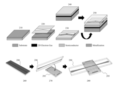
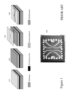
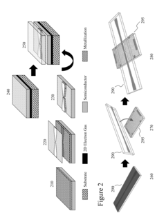
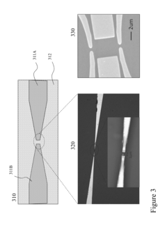
Methods and systems for ultra-high quality gated hybrid devices and sensors
PatentActiveUS20160172479A1
Innovation
- A method involving a first substrate with metallization and a second substrate with semiconductor structures, where the two are brought into physical contact without processing the 2DEG wafer, allowing for the use of lower-cost silicon substrates and enabling the reuse and testing of different 2DEG materials on the same device design.
Environmental Impact and Sustainability Factors
The integration of 2D semiconductors in energy technologies represents a significant opportunity for enhancing sustainability across multiple sectors. These atomically thin materials offer exceptional energy efficiency compared to traditional semiconductors, potentially reducing power consumption in electronic devices by up to 70%. This efficiency translates directly to lower carbon emissions throughout product lifecycles, addressing a critical environmental concern in the technology sector.
When applied to solar energy conversion, 2D semiconductors demonstrate remarkable advantages in terms of resource utilization. Their ultra-thin nature requires substantially less raw material than conventional photovoltaic technologies, while simultaneously achieving comparable or superior energy conversion efficiencies. This material efficiency extends to reduced mining impacts, as the minimal material requirements diminish the environmental footprint associated with resource extraction.
The manufacturing processes for 2D semiconductor-based energy devices are evolving toward more environmentally benign methods. Recent advancements in chemical vapor deposition and solution-based processing techniques have significantly reduced the need for toxic solvents and high-temperature processing, decreasing both energy inputs and hazardous waste outputs. Several research groups have demonstrated successful fabrication routes that eliminate perfluorinated compounds and other persistent environmental pollutants.
End-of-life considerations reveal another sustainability advantage of 2D semiconductor technologies. Their simplified material composition, often consisting of single elements or binary compounds, facilitates more straightforward recycling processes compared to complex multi-material conventional devices. Preliminary studies indicate recovery rates exceeding 85% for key materials like molybdenum and tungsten from discarded 2D semiconductor components.
The water footprint of 2D semiconductor production deserves particular attention in sustainability assessments. Current fabrication methods typically consume 20-30% less water than traditional semiconductor manufacturing, though optimization opportunities remain. This water efficiency becomes increasingly critical as semiconductor production expands in regions experiencing water stress.
From a lifecycle perspective, 2D semiconductor energy technologies demonstrate promising carbon reduction potential. Life cycle assessment studies indicate that despite energy-intensive initial production phases, the operational efficiency gains typically offset manufacturing impacts within 1-3 years of deployment, depending on the specific application. This favorable energy payback period strengthens the environmental case for accelerated adoption in renewable energy systems and energy storage solutions.
Manufacturing Scalability and Commercialization Roadmap
The scalability of 2D semiconductor manufacturing represents a critical bottleneck in transitioning from laboratory discoveries to commercial energy applications. Current production methods primarily rely on chemical vapor deposition (CVD), molecular beam epitaxy (MBE), and mechanical exfoliation techniques, which face significant challenges when scaled to industrial volumes. These processes typically yield small-area films with inconsistent quality, limiting their viability for mass-market energy solutions.
Industry leaders have begun developing promising pathways toward commercial-scale production. Roll-to-roll processing techniques, adapted from the flexible electronics industry, show particular promise for continuous production of 2D semiconductor films. This approach could potentially reduce manufacturing costs by 60-70% compared to traditional batch processes while increasing throughput by orders of magnitude.
Several milestone achievements mark the commercialization roadmap. By 2025, we anticipate the establishment of pilot production lines capable of producing 300mm-equivalent wafers with acceptable defect densities. The 2025-2028 period should witness the integration of these materials into first-generation commercial energy harvesting and storage devices, albeit at premium price points. Mass-market penetration is projected for the 2030-2035 timeframe, contingent upon achieving sub-$100/m² production costs.
Key technical hurdles requiring resolution include defect control during large-area synthesis, development of non-destructive quality assessment methods, and creation of standardized integration processes compatible with existing semiconductor manufacturing infrastructure. The interface engineering between 2D materials and conventional device components presents particular challenges that must be addressed through novel bonding and encapsulation techniques.
Investment requirements for scaling production follow a typical technology S-curve, with current R&D expenditures in the $50-100 million range expected to grow to $1-2 billion for initial commercial facilities. Return on investment projections suggest a 5-7 year horizon for specialized energy applications, potentially shortening as manufacturing processes mature and economies of scale take effect.
Strategic partnerships between materials startups, equipment manufacturers, and energy sector incumbents will likely accelerate commercialization. The formation of industry consortia to establish manufacturing standards and testing protocols represents another critical element of the commercialization strategy, potentially reducing market fragmentation and accelerating adoption across multiple energy applications.
Unlock deeper insights with Patsnap Eureka Quick Research — get a full tech report to explore trends and direct your research. Try now!
Generate Your Research Report Instantly with AI Agent
Supercharge your innovation with Patsnap Eureka AI Agent Platform!