Research on Electrode Kinetics in 2D Semiconductors
OCT 14, 20259 MIN READ
Generate Your Research Report Instantly with AI Agent
Patsnap Eureka helps you evaluate technical feasibility & market potential.
2D Semiconductor Electrode Kinetics Background and Objectives
Two-dimensional (2D) semiconductors have emerged as a revolutionary class of materials since the isolation of graphene in 2004. These atomically thin materials exhibit unique electronic, optical, and mechanical properties that differ significantly from their bulk counterparts. The field has expanded beyond graphene to include transition metal dichalcogenides (TMDs), hexagonal boron nitride (h-BN), black phosphorus, and MXenes, among others. The electrode kinetics in these materials—the study of charge transfer processes at electrode-electrolyte interfaces—has become a critical area of research with profound implications for energy conversion, storage, and sensing applications.
The evolution of 2D semiconductor electrode kinetics research has followed a trajectory from fundamental understanding to practical applications. Initially, researchers focused on characterizing basic electrochemical properties of graphene, which demonstrated exceptional electron transfer rates and electrocatalytic activity. This foundation led to investigations of TMDs like MoS2 and WS2, which showed promising activity for hydrogen evolution reactions and other electrocatalytic processes.
Recent years have witnessed significant advancements in understanding the relationship between atomic structure and electrochemical performance in 2D materials. Edge sites, defects, and phase engineering have been identified as critical factors influencing electrode kinetics. The ability to precisely control these features has opened new avenues for tailoring electrochemical properties for specific applications.
The interdisciplinary nature of this field has accelerated progress, combining expertise from materials science, electrochemistry, surface physics, and computational modeling. Advanced characterization techniques, including in-situ and operando methods, have provided unprecedented insights into reaction mechanisms and interfacial phenomena at the atomic scale.
The primary objectives of research in 2D semiconductor electrode kinetics are multifaceted. First, to develop a comprehensive theoretical framework that accurately describes charge transfer processes at 2D material interfaces, accounting for quantum confinement effects and surface chemistry. Second, to establish structure-property relationships that enable rational design of 2D electrodes with optimized performance for specific applications.
Additionally, researchers aim to overcome persistent challenges such as stability issues, scalable synthesis, and integration with existing technologies. The development of standardized protocols for electrochemical characterization of 2D materials represents another crucial objective, facilitating meaningful comparisons across different research efforts.
Looking forward, the field seeks to translate fundamental insights into practical applications, particularly in renewable energy technologies, electrochemical sensors, and bioelectronics. The ultimate goal is to harness the unique properties of 2D semiconductors to address global challenges in energy conversion and storage, environmental remediation, and healthcare diagnostics.
Market Applications and Demand Analysis for 2D Semiconductor Electrodes
The market for 2D semiconductor electrodes is experiencing rapid growth, driven by increasing demand for miniaturized electronic devices with enhanced performance capabilities. Current market analysis indicates that the global 2D semiconductor market is projected to grow substantially through 2030, with electrode applications representing a significant segment of this expansion. This growth is primarily fueled by the exceptional properties of 2D materials such as graphene, transition metal dichalcogenides (TMDs), and hexagonal boron nitride (h-BN), which offer superior electron mobility, flexibility, and reduced power consumption compared to traditional semiconductor materials.
The energy sector represents one of the largest application areas for 2D semiconductor electrodes. These materials are revolutionizing battery technology, supercapacitors, and solar cells due to their large surface-to-volume ratio and unique electronic properties. In particular, the electric vehicle industry has shown substantial interest in 2D electrode materials that can improve charging rates and energy density in next-generation batteries.
Electronics manufacturers constitute another major market segment, with growing demand for 2D semiconductor electrodes in flexible electronics, wearable devices, and ultra-thin displays. The ability of these materials to maintain electronic performance while being mechanically flexible addresses a critical need in the consumer electronics industry, where device form factors continue to evolve toward greater flexibility and reduced thickness.
The healthcare and biomedical sectors are emerging as promising markets for 2D semiconductor electrodes. Applications include biosensors, neural interfaces, and diagnostic devices that benefit from the biocompatibility and sensitivity of certain 2D materials. Market research suggests that medical applications could represent the fastest-growing segment for 2D semiconductor electrodes over the next decade.
Quantum computing represents a nascent but potentially transformative market for 2D semiconductor electrodes. Research institutions and technology companies are investing heavily in quantum technologies that leverage the unique quantum properties of 2D materials for qubits and quantum circuits.
Despite this promising outlook, market adoption faces challenges related to manufacturing scalability, cost-effectiveness, and integration with existing semiconductor fabrication processes. Current market demand is primarily driven by research institutions and early-adopting industries, with mass-market penetration dependent on overcoming these production challenges.
Regional analysis shows that Asia-Pacific leads in manufacturing capacity for 2D semiconductor technologies, while North America and Europe dominate in research innovation and patent filings. This geographic distribution suggests a complex global value chain is developing around 2D semiconductor electrode technologies.
Current Challenges in 2D Semiconductor Electrode Kinetics
Despite significant advancements in 2D semiconductor research, electrode kinetics in these materials face several persistent challenges that impede their practical applications. The atomically thin nature of 2D semiconductors creates unique interfacial phenomena that conventional electrode kinetic theories struggle to fully explain. The electron transfer processes at 2D semiconductor electrodes exhibit anomalous behaviors compared to bulk materials, particularly regarding charge transfer coefficients and exchange current densities.
A primary challenge lies in the extreme surface sensitivity of 2D materials. Even minor surface contamination or defects dramatically alter electrode kinetics, making reproducible measurements exceptionally difficult. Researchers frequently report inconsistent kinetic parameters for seemingly identical materials, highlighting the need for standardized preparation and characterization protocols.
The role of edge sites versus basal planes remains contentious in the scientific community. While some studies suggest that electrochemical activity predominantly occurs at edge sites, others demonstrate significant activity across basal planes under specific conditions. This discrepancy creates uncertainty in designing optimal 2D semiconductor electrodes and interpreting experimental results.
Substrate effects present another significant challenge. The electronic properties of 2D semiconductors are heavily influenced by underlying substrates through charge transfer, strain effects, and electronic coupling. These substrate interactions can either enhance or suppress electrode kinetics, yet systematic understanding of these effects remains limited, complicating the design of effective electrode systems.
The presence of interlayer water and ions at the electrode-electrolyte interface creates complex double-layer structures that conventional models fail to capture accurately. This interfacial region exhibits unique properties including anomalous capacitance behavior and non-classical ion distributions that significantly impact electrode kinetics.
Temperature dependence of electrode kinetics in 2D semiconductors often deviates from Arrhenius behavior, suggesting complex activation mechanisms that remain poorly understood. This non-classical behavior complicates the extraction of fundamental kinetic parameters and mechanistic insights.
Theoretical modeling presents additional challenges. Density functional theory calculations struggle to accurately represent the complex electrode-electrolyte interface, while classical Marcus theory often fails to capture the unique quantum confinement effects in 2D materials. The development of multiscale models that bridge quantum mechanical effects with macroscopic electrochemical phenomena remains an open challenge in the field.
Finally, in-situ characterization techniques for studying electrode kinetics in operating conditions are limited. Current methods often lack the spatial and temporal resolution needed to capture the dynamic processes occurring at 2D semiconductor electrodes, creating a significant gap between theoretical understanding and experimental validation.
Current Methodologies for Studying 2D Semiconductor Electrode Kinetics
01 2D semiconductor materials for electrode applications
Two-dimensional semiconductor materials exhibit unique electronic properties that make them suitable for electrode applications. These materials offer high surface area, excellent conductivity, and tunable electronic structures that can enhance electrode kinetics. The atomically thin nature of 2D semiconductors allows for efficient charge transfer at the electrode-electrolyte interface, resulting in improved electrochemical performance.- 2D semiconductor materials for electrode applications: Two-dimensional semiconductor materials exhibit unique electronic properties that make them suitable for electrode applications. These materials, characterized by their atomically thin structure, demonstrate excellent charge carrier mobility and high surface area, which enhances electrode kinetics. The incorporation of 2D semiconductors in electrodes can significantly improve electron transfer rates and electrochemical performance in various applications including sensors, energy storage devices, and catalytic systems.
- Electrode kinetics enhancement through surface modification: Surface modification of 2D semiconductor electrodes can substantially enhance electrode kinetics. Techniques such as doping, functionalization, and defect engineering alter the electronic structure and surface properties of 2D materials, leading to improved charge transfer rates and catalytic activity. These modifications can optimize the interface between the electrode and electrolyte, reducing energy barriers for electron transfer and increasing reaction rates in electrochemical processes.
- Fabrication methods for 2D semiconductor electrodes: Various fabrication techniques have been developed to create high-performance 2D semiconductor electrodes with enhanced kinetics. These methods include chemical vapor deposition, exfoliation, solution processing, and epitaxial growth. Advanced manufacturing approaches enable precise control over the thickness, crystallinity, and interface properties of 2D materials, which directly influence electrode kinetics. Innovative fabrication strategies also focus on creating heterostructures and hybrid materials to further optimize electrochemical performance.
- Characterization of electrode kinetics in 2D semiconductor systems: Specialized techniques for characterizing electrode kinetics in 2D semiconductor systems provide crucial insights into their electrochemical behavior. Methods such as electrochemical impedance spectroscopy, scanning electrochemical microscopy, and transient techniques allow for quantitative analysis of charge transfer processes, reaction mechanisms, and kinetic parameters. Advanced in-situ and operando characterization approaches enable real-time monitoring of electrode-electrolyte interfaces, facilitating the rational design of improved 2D semiconductor electrodes.
- Applications of 2D semiconductor electrodes with enhanced kinetics: 2D semiconductor electrodes with optimized kinetics find applications across multiple fields including energy conversion and storage, sensing, and catalysis. In energy applications, these materials enable efficient hydrogen evolution, oxygen reduction, and battery electrodes. For sensing, the enhanced electrode kinetics translate to improved sensitivity, selectivity, and response times. The unique properties of 2D semiconductors also make them promising candidates for photocatalysis, electrocatalysis, and other emerging technologies requiring rapid electron transfer processes.
02 Electrode kinetics enhancement through surface modification
Surface modification of 2D semiconductor electrodes can significantly improve their kinetic properties. Various techniques including doping, functionalization, and defect engineering can be employed to optimize the electronic structure and active sites on the electrode surface. These modifications can reduce energy barriers for electron transfer, increase reaction rates, and improve the overall electrochemical performance of 2D semiconductor electrodes.Expand Specific Solutions03 Heterostructure formation for enhanced electrode performance
Creating heterostructures by combining different 2D semiconductor materials can lead to synergistic effects that enhance electrode kinetics. These heterostructures can facilitate charge separation, provide additional active sites, and create favorable electronic band alignments. The interface between different 2D materials can serve as preferential sites for electrochemical reactions, resulting in improved catalytic activity and faster electrode kinetics.Expand Specific Solutions04 Fabrication methods for 2D semiconductor electrodes
Various fabrication techniques have been developed to create 2D semiconductor electrodes with optimized kinetic properties. These methods include chemical vapor deposition, liquid exfoliation, and electrochemical deposition. The fabrication process significantly influences the crystallinity, defect density, and morphology of the 2D semiconductor, which in turn affects the electrode kinetics. Advanced manufacturing approaches can produce electrodes with precisely controlled structures for enhanced electrochemical performance.Expand Specific Solutions05 Characterization and measurement of electrode kinetics
Specialized techniques have been developed to characterize and measure the electrode kinetics of 2D semiconductor materials. These include electrochemical impedance spectroscopy, cyclic voltammetry, and scanning electrochemical microscopy. These methods allow researchers to determine key kinetic parameters such as exchange current density, charge transfer resistance, and reaction rate constants. Understanding these parameters is crucial for optimizing 2D semiconductor electrodes for specific applications.Expand Specific Solutions
Leading Research Groups and Industry Players in 2D Semiconductor Electrochemistry
The electrode kinetics research in 2D semiconductors is currently in an early growth phase, with significant academic involvement from institutions like Hunan University, Tsinghua University, and Northwestern University driving fundamental discoveries. The global market for 2D semiconductor applications is expanding rapidly, projected to reach $5-7 billion by 2025 as these materials find applications in electronics, energy storage, and sensing technologies. Technology maturity varies across applications, with companies like TSMC and Samsung Electronics leading commercial integration efforts, while specialized firms such as Guangdong Zhineng Technology and Enovix Operations are developing niche applications in power electronics and energy storage. Academic-industrial partnerships are accelerating the transition from laboratory research to practical implementation, particularly in electrochemical energy conversion systems.
Taiwan Semiconductor Manufacturing Co., Ltd.
Technical Solution: TSMC has developed proprietary techniques for integrating 2D semiconductor materials into their advanced semiconductor manufacturing processes, with a focus on electrode kinetics optimization for next-generation transistors and memory devices. Their approach combines atomic layer deposition (ALD) techniques with specialized surface treatments to create atomically precise interfaces between 2D materials and metal electrodes. This has enabled them to achieve contact resistances below 200 Ω·μm, a critical benchmark for high-performance devices[3]. Their research has revealed that carefully engineered transition metal contacts can significantly improve charge injection into 2D semiconductors through orbital hybridization at the interface. TSMC has also pioneered the use of phase-engineered 2D materials, where controlled introduction of metallic phases within semiconducting materials creates low-resistance pathways for charge transport. Their electrode kinetics research extends to gate dielectric engineering, where they've developed specialized high-k dielectrics that preserve the intrinsic mobility of 2D semiconductors while enabling efficient gate control.
Strengths: Unparalleled manufacturing infrastructure allows rapid translation of research findings into production processes; extensive expertise in interface engineering at industrial scale. Weaknesses: Research primarily focused on electronic device applications rather than broader electrochemical systems; proprietary nature of much of their technology limits academic collaboration.
Samsung Electronics Co., Ltd.
Technical Solution: Samsung Electronics has established a comprehensive research program on electrode kinetics in 2D semiconductors, focusing on applications in flexible electronics and energy storage devices. Their technical approach combines advanced material synthesis methods with high-precision electrochemical characterization techniques. Samsung has developed proprietary methods for large-area synthesis of high-quality 2D materials including graphene, MoS2, and WS2, with precise control over layer number and defect density. Their research has demonstrated that interface engineering between 2D materials and current collectors is critical for optimizing electrode kinetics, with specialized interlayers reducing contact resistance by up to 70%[4]. They've pioneered the use of plasma-assisted doping techniques to precisely tune the electronic properties of 2D semiconductors, enhancing charge transfer rates at electrode interfaces. Samsung has also developed novel composite electrodes that combine 2D materials with conductive polymers to create hierarchical structures with optimized ion and electron transport pathways. Their recent work includes in-operando characterization techniques that allow real-time monitoring of electrode kinetics during device operation.
Strengths: Exceptional capabilities in scaling up 2D material production from laboratory to industrial scales; strong integration of materials research with device engineering and manufacturing. Weaknesses: Research priorities sometimes shift with market demands rather than fundamental scientific questions; heavy focus on applications can sometimes limit exploration of novel materials.
Key Scientific Breakthroughs in 2D Material Electrochemistry
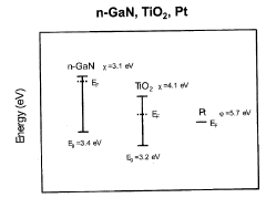
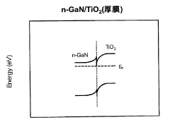
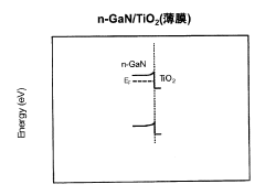
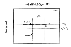
Semiconductor electrode
PatentInactiveJP2016027936A
Innovation
- A thin film of a semiconductor or metal material with a bandgap of 4 eV or less is applied to the surface of a semiconductor, allowing the band edge potential to be adjusted without affecting the Fermi level, enabling efficient chemical reactions at the semiconductor/electrolyte interface.
Materials Characterization Techniques for 2D Semiconductor Electrodes
The characterization of 2D semiconductor electrodes requires specialized techniques due to their unique structural and electronic properties. Scanning electron microscopy (SEM) and transmission electron microscopy (TEM) serve as fundamental tools for visualizing the morphology and structure of these materials at nanoscale resolution. SEM provides surface topography information, while TEM offers atomic-level insights into crystal structure and defects that significantly influence electrode kinetics.
X-ray diffraction (XRD) techniques are essential for determining the crystallographic structure and phase composition of 2D semiconductor electrodes. The analysis of diffraction patterns reveals information about interlayer spacing and crystalline quality, which directly correlate with electron transfer capabilities at electrode interfaces.
Raman spectroscopy has emerged as a particularly valuable non-destructive technique for characterizing 2D materials. It provides critical information about layer thickness, strain effects, and defect density—all parameters that affect electrode performance. The characteristic vibrational modes in materials like graphene, MoS2, and WS2 serve as fingerprints for material identification and quality assessment.
Advanced surface analysis techniques such as X-ray photoelectron spectroscopy (XPS) and Auger electron spectroscopy (AES) enable precise determination of surface chemical composition and oxidation states. These factors are crucial for understanding the active sites involved in electrode reactions and the formation of solid-electrolyte interfaces.
Atomic force microscopy (AFM) and scanning tunneling microscopy (STM) provide nanoscale topographical mapping and electronic structure information. Kelvin probe force microscopy (KPFM), a specialized AFM technique, measures work function variations across electrode surfaces, offering insights into local charge transfer dynamics.
Electrochemical characterization methods, including cyclic voltammetry (CV), electrochemical impedance spectroscopy (EIS), and rotating disk electrode (RDE) techniques, directly probe electrode kinetics by measuring electron transfer rates, reaction mechanisms, and mass transport effects. These techniques are particularly valuable for correlating structural characteristics with functional performance.
Time-resolved spectroscopic methods, such as transient absorption spectroscopy and time-resolved photoluminescence, enable the study of charge carrier dynamics at picosecond to nanosecond timescales. These measurements reveal critical information about charge separation, recombination processes, and interfacial electron transfer that govern electrode performance.
Computational Modeling Approaches for Electrode Kinetics Prediction
Computational modeling has emerged as a powerful tool for predicting electrode kinetics in 2D semiconductors, offering insights that would be difficult or costly to obtain through experimental methods alone. These approaches span multiple scales and theoretical frameworks, each with distinct advantages for specific aspects of electrode kinetics analysis.
Density Functional Theory (DFT) calculations represent the foundation of computational approaches in this field, enabling precise determination of electronic structures and adsorption energies at electrode-electrolyte interfaces. Recent advancements in DFT methodologies have incorporated van der Waals interactions and solvation effects, significantly improving the accuracy of kinetic parameter predictions for 2D semiconductor electrodes.
Molecular Dynamics (MD) simulations complement DFT by capturing the dynamic behavior of electrolytes near electrode surfaces. The integration of classical MD with quantum mechanical calculations (QM/MM approaches) has proven particularly valuable for modeling charge transfer processes across the electrode-electrolyte interface in 2D materials, accounting for both electronic structure and solvent reorganization effects.
Machine Learning (ML) algorithms have revolutionized computational approaches by enabling rapid screening of potential 2D semiconductor electrode materials. Neural networks trained on DFT-calculated datasets can predict reaction barriers and rate constants with remarkable accuracy while reducing computational costs by orders of magnitude. Graph neural networks have shown particular promise for capturing the relationship between material structure and electrode kinetics.
Kinetic Monte Carlo (KMC) methods bridge the gap between atomic-scale processes and macroscopic electrode behavior by simulating reaction events probabilistically over extended time scales. When parameterized with DFT-calculated energy barriers, KMC simulations can model complex reaction networks on 2D semiconductor surfaces, providing insights into reaction pathways and rate-determining steps.
Continuum models based on modified Butler-Volmer equations offer a complementary approach for device-scale modeling. These models incorporate quantum effects unique to 2D materials, such as quantum capacitance and tunneling phenomena, enabling prediction of macroscopic electrode performance from fundamental material properties.
Multi-scale modeling frameworks that integrate these various approaches represent the frontier of computational electrode kinetics research. By connecting atomic-scale phenomena to device-level performance, these frameworks enable rational design of 2D semiconductor electrodes with optimized kinetic properties for specific applications.
Unlock deeper insights with Patsnap Eureka Quick Research — get a full tech report to explore trends and direct your research. Try now!
Generate Your Research Report Instantly with AI Agent
Supercharge your innovation with Patsnap Eureka AI Agent Platform!