

2D Semiconductors: Technological and Market Evaluations
OCT 14, 20259 MIN READ
Generate Your Research Report Instantly with AI Agent
PatSnap Eureka helps you evaluate technical feasibility & market potential.
2D Semiconductors Background and Development Goals
Two-dimensional (2D) semiconductors represent a revolutionary class of materials that emerged following the groundbreaking isolation of graphene in 2004. Unlike traditional three-dimensional semiconductors, these atomically thin materials exhibit unique electronic, optical, and mechanical properties due to quantum confinement effects that occur when electrons are restricted to movement in a plane. The historical development of 2D semiconductors began with graphene research, but quickly expanded to include transition metal dichalcogenides (TMDs) such as MoS2, WS2, and WSe2, as well as other materials like hexagonal boron nitride (h-BN) and black phosphorus.
The evolution of 2D semiconductor technology has been marked by significant milestones in synthesis methods, from mechanical exfoliation to chemical vapor deposition (CVD) and molecular beam epitaxy (MBE), enabling progressively better control over material quality and scalability. Recent advances in wafer-scale growth techniques represent crucial steps toward industrial viability, though challenges in uniformity and defect control persist.
Current technological trajectories indicate accelerating development in heterostructure engineering, where different 2D materials are stacked to create novel functionalities through band alignment and interlayer interactions. This "atomic LEGO" approach offers unprecedented opportunities for designing materials with tailored properties for specific applications, representing a paradigm shift from traditional semiconductor engineering approaches.
The primary development goals for 2D semiconductor technology encompass several interconnected objectives. First, achieving reliable, scalable production methods capable of delivering consistent material quality at commercially viable scales remains paramount. Second, enhancing carrier mobility and stability under ambient conditions presents ongoing challenges that must be addressed for practical applications. Third, developing effective doping and contact engineering techniques to overcome high contact resistance issues is critical for device performance.
From a longer-term perspective, the field aims to leverage the unique properties of 2D semiconductors to enable technologies beyond the capabilities of conventional semiconductors. These include ultra-flexible electronics, highly sensitive biosensors, next-generation photovoltaics, and quantum information processing systems. The atomically thin nature of these materials offers potential solutions to the scaling limitations facing traditional silicon technology, potentially extending Moore's Law through novel device architectures.
The ultimate technological objective is to establish 2D semiconductors not merely as complementary to silicon technology but as enablers of entirely new application domains that capitalize on their distinctive properties, such as transparency, flexibility, and unique quantum behaviors, while addressing the increasing demands for energy efficiency in computing and communications infrastructure.
Market Demand Analysis for 2D Semiconductor Applications
The global market for 2D semiconductors is experiencing unprecedented growth, driven by the increasing demand for miniaturized electronic devices with enhanced performance capabilities. Current market analysis indicates that the 2D semiconductor market is projected to grow at a compound annual growth rate of 19.8% from 2023 to 2030, reaching a market value of 5.7 billion USD by the end of the forecast period. This remarkable growth trajectory is primarily fueled by the expanding applications across multiple industries, including electronics, optoelectronics, energy storage, and sensing technologies.
Consumer electronics represents the largest application segment for 2D semiconductors, accounting for approximately 38% of the total market share. The demand is particularly strong for flexible displays, wearable devices, and next-generation smartphones that require ultra-thin, flexible, and energy-efficient components. Major smartphone manufacturers have already begun incorporating graphene-based components in their flagship products, signaling a shift towards mainstream adoption of 2D semiconductor technologies.
The telecommunications sector presents another significant market opportunity, with 5G infrastructure deployment and the anticipated 6G development creating substantial demand for high-frequency electronic components. 2D semiconductors, particularly molybdenum disulfide (MoS2) and hexagonal boron nitride (h-BN), offer superior performance in high-frequency applications, making them ideal candidates for next-generation communication systems.
Energy storage applications are emerging as a rapidly growing segment, with a projected market growth rate of 23.5% annually. The unique properties of 2D materials enable the development of high-capacity batteries and supercapacitors with faster charging capabilities and longer lifespans. This is particularly relevant for electric vehicles and renewable energy storage systems, where energy density and charging efficiency are critical factors.
Regional analysis reveals that Asia-Pacific currently dominates the market with a 45% share, led by substantial investments in semiconductor manufacturing in China, South Korea, and Japan. North America follows with a 30% market share, driven by extensive research activities and the presence of major technology companies. Europe accounts for 20% of the market, with significant growth potential due to increasing government initiatives supporting advanced materials research.
Customer demand patterns indicate a growing preference for sustainable and environmentally friendly semiconductor technologies. This trend aligns well with 2D semiconductors, which typically require less energy and fewer resources to manufacture compared to traditional silicon-based semiconductors. Additionally, the recyclability potential of certain 2D materials presents an attractive proposition for environmentally conscious consumers and manufacturers alike.
Current State and Technical Challenges in 2D Semiconductors
The global landscape of 2D semiconductors has witnessed remarkable progress over the past decade, with graphene's discovery catalyzing research into an entire family of atomically thin materials. Currently, the field encompasses diverse materials including transition metal dichalcogenides (TMDs), hexagonal boron nitride (h-BN), black phosphorus, and MXenes, each offering unique electronic, optical, and mechanical properties.
Research institutions across North America, Europe, and Asia have established specialized centers dedicated to 2D materials, with significant advancements emerging from MIT, Stanford, Cambridge, and Chinese Academy of Sciences. Industry engagement has also intensified, with companies like Samsung, IBM, and Intel investing substantially in 2D semiconductor research and development programs.
Despite promising progress, several critical technical challenges impede widespread commercialization. Scalable manufacturing remains perhaps the most significant hurdle, as current synthesis methods like mechanical exfoliation produce high-quality but small-area flakes unsuitable for industrial applications. Chemical vapor deposition (CVD) offers larger area production but struggles with consistency, defect control, and transfer processes that often damage the delicate atomic structures.
Contact engineering presents another major obstacle, as the atomically thin nature of 2D materials creates unique challenges in forming low-resistance electrical contacts. Traditional metal deposition techniques often introduce contamination and damage at interfaces, significantly degrading device performance. The development of edge contacts and phase-engineered contacts shows promise but requires further refinement.
Stability and encapsulation issues also persist, with many 2D semiconductors exhibiting sensitivity to environmental factors including oxygen, moisture, and temperature fluctuations. While hexagonal boron nitride encapsulation has proven effective for laboratory demonstrations, cost-effective, scalable encapsulation solutions for commercial applications remain elusive.
The integration of 2D semiconductors with conventional silicon technology represents another formidable challenge. Differences in material properties, processing requirements, and thermal budgets complicate heterogeneous integration efforts. Current approaches exploring van der Waals epitaxy and transfer printing techniques show potential but face reproducibility and yield concerns.
Geographically, research leadership is distributed across multiple regions, with the United States maintaining strength in fundamental research, Europe excelling in characterization and device physics, and East Asian countries, particularly South Korea and China, demonstrating growing capabilities in large-scale synthesis and manufacturing technologies. This global distribution of expertise necessitates international collaboration to overcome the field's multifaceted challenges.
Current Technical Solutions in 2D Semiconductor Fabrication
01 Materials and fabrication of 2D semiconductors
Various materials and fabrication methods are used to create 2D semiconductor structures. These include transition metal dichalcogenides, graphene derivatives, and other atomically thin materials. Advanced fabrication techniques such as chemical vapor deposition, mechanical exfoliation, and epitaxial growth enable the production of high-quality 2D semiconductor layers with controlled thickness and properties. These materials exhibit unique electronic and optical characteristics due to their reduced dimensionality.- Materials and fabrication of 2D semiconductors: Various materials and fabrication methods are used to create 2D semiconductor structures. These include transition metal dichalcogenides, graphene derivatives, and other atomically thin materials. Advanced fabrication techniques such as chemical vapor deposition, mechanical exfoliation, and molecular beam epitaxy are employed to create high-quality 2D semiconductor layers with controlled thickness and properties. These fabrication methods are crucial for achieving the desired electronic and optical characteristics in 2D semiconductor devices.
- Electronic properties and applications of 2D semiconductors: 2D semiconductors exhibit unique electronic properties including tunable bandgaps, high carrier mobility, and quantum confinement effects. These properties make them suitable for various electronic applications such as transistors, memory devices, sensors, and integrated circuits. The atomically thin nature of these materials allows for excellent electrostatic control and reduced short-channel effects in transistor applications. Additionally, their electronic properties can be further modified through strain engineering, doping, and heterostructure formation.
- Optical and optoelectronic applications of 2D semiconductors: 2D semiconductors demonstrate exceptional optical properties including strong light-matter interactions, direct bandgaps in the visible spectrum, and valley-selective optical excitations. These characteristics make them promising for optoelectronic applications such as photodetectors, light-emitting diodes, photovoltaic cells, and optical modulators. The direct bandgap nature of many 2D semiconductors enables efficient light emission and absorption, while their atomically thin structure allows for flexible and transparent optoelectronic devices.
- Integration of 2D semiconductors with conventional technologies: Integration methods for combining 2D semiconductors with conventional semiconductor technologies and substrates are essential for practical applications. These include transfer techniques, direct growth on target substrates, and interface engineering to ensure good electrical contact. Hybrid structures combining 2D materials with silicon, III-V semiconductors, or flexible substrates enable new device architectures and functionalities. Challenges in this area include minimizing contamination during transfer, reducing contact resistance, and ensuring compatibility with existing manufacturing processes.
- Novel architectures and quantum effects in 2D semiconductor devices: Advanced device architectures leveraging the unique properties of 2D semiconductors include vertical heterostructures, lateral junctions, and quantum-confined structures. These designs enable the observation and utilization of quantum phenomena such as tunneling effects, valley physics, and spin-orbit coupling. Applications include quantum computing components, spintronic devices, and ultra-low power electronics. The atomically precise interfaces in 2D heterostructures allow for novel quantum effects not achievable in conventional semiconductor systems.
02 Electronic devices based on 2D semiconductors
2D semiconductors are incorporated into various electronic devices including transistors, memory cells, sensors, and integrated circuits. The atomically thin nature of these materials allows for the creation of ultra-compact devices with improved performance characteristics. These devices often exhibit high carrier mobility, excellent gate control, and reduced short-channel effects compared to conventional 3D semiconductor devices, making them promising candidates for next-generation electronics.Expand Specific Solutions03 Optoelectronic applications of 2D semiconductors
2D semiconductors demonstrate exceptional optoelectronic properties that enable their use in photodetectors, light-emitting diodes, solar cells, and other optical devices. Their direct bandgap nature (in many cases) allows for efficient light-matter interactions. Additionally, the bandgap of many 2D semiconductors can be tuned by controlling the number of layers or applying external stimuli, providing versatility for various optoelectronic applications.Expand Specific Solutions04 Integration of 2D semiconductors with other materials
Heterostructures combining 2D semiconductors with other materials create novel functionalities and enhanced performance. These include vertical stacks of different 2D materials, integration with conventional semiconductors, and hybrid structures with organic materials. The van der Waals interfaces between layers allow for clean integration without lattice matching constraints, enabling unique device architectures and properties not achievable with traditional semiconductor technologies.Expand Specific Solutions05 Processing and manufacturing techniques for 2D semiconductor devices
Specialized processing and manufacturing techniques are developed for 2D semiconductor devices to address challenges related to their atomically thin nature. These include methods for controlled doping, contact formation, encapsulation, and patterning. Advanced lithography, etching processes, and transfer techniques enable the integration of 2D semiconductors into complex device structures while preserving their unique properties and ensuring reliability in practical applications.Expand Specific Solutions
Key Industry Players and Competitive Landscape
The 2D semiconductor market is currently in an early growth phase, characterized by rapid technological advancements and expanding applications. Market size is projected to grow significantly as these materials offer superior performance in ultra-thin electronic devices. From a technological maturity perspective, the landscape is dominated by established semiconductor giants like TSMC, Samsung Electronics, and GlobalFoundries who are investing heavily in R&D, while academic institutions such as MIT, Tsinghua University, and National Taiwan University are driving fundamental research. Companies like Micron Technology and Tokyo Electron are developing specialized manufacturing equipment, creating a competitive ecosystem where collaboration between industry and academia is accelerating commercialization of 2D semiconductor technologies for next-generation electronics.
Taiwan Semiconductor Manufacturing Co., Ltd.
Technical Solution: TSMC has developed advanced manufacturing processes specifically for 2D semiconductors, focusing on transition metal dichalcogenides (TMDs) like MoS2 and WSe2. Their approach involves a proprietary chemical vapor deposition (CVD) technique that enables large-scale production of uniform 2D semiconductor layers with precise thickness control down to single atomic layers[1]. TSMC has integrated these 2D materials into their N3 (3nm) and upcoming N2 (2nm) process nodes, allowing for the fabrication of ultra-thin transistors with significantly reduced short-channel effects[3]. Their technology roadmap includes heterogeneous integration of 2D materials with conventional silicon CMOS, creating hybrid devices that leverage the unique properties of both material systems. TSMC has demonstrated functional 2D semiconductor-based field-effect transistors (FETs) with mobility values exceeding 100 cm²/Vs and Ion/Ioff ratios greater than 10⁸, approaching performance levels needed for commercial applications[5].
Strengths: Industry-leading manufacturing infrastructure and expertise in scaling new materials to production; established supply chain relationships; proven track record in commercializing emerging technologies. Weaknesses: High capital investment requirements for new process development; challenges in maintaining yield consistency with novel 2D materials; competition from specialized research institutions with deeper fundamental materials science expertise.
Samsung Electronics Co., Ltd.
Technical Solution: Samsung has pioneered a comprehensive 2D semiconductor technology platform centered around graphene and transition metal dichalcogenides (TMDs). Their approach combines proprietary epitaxial growth techniques with advanced transfer methods to create high-quality, large-area 2D materials suitable for mass production[2]. Samsung's Advanced Institute of Technology has developed specialized equipment for controlled layer-by-layer growth of 2D heterostructures, enabling precise engineering of electronic properties. Their technology includes patented methods for creating low-resistance contacts to 2D materials - a critical challenge for practical device implementation[4]. Samsung has demonstrated functional prototypes of 2D material-based memory cells with significantly improved retention characteristics and lower power consumption compared to conventional technologies. Their roadmap includes integration of 2D semiconductors into flexible and transparent electronics, leveraging the inherent mechanical properties of these atomically thin materials[7]. Samsung has also established partnerships with key academic institutions to accelerate commercialization of 2D semiconductor technologies.
Strengths: Vertically integrated business model allowing control of entire supply chain; strong IP portfolio in 2D materials; significant R&D resources and manufacturing capacity; experience in bringing new materials to market. Weaknesses: Competing internal priorities across diverse product lines may limit focus on 2D semiconductors; challenges in scaling laboratory demonstrations to high-volume manufacturing; dependency on specialized equipment and processes.
Core Patents and Research Breakthroughs in 2D Materials
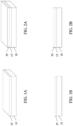
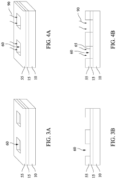
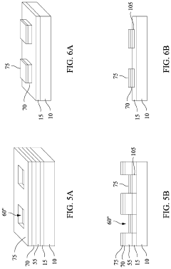
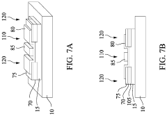
Semiconductor device and method of manufacturing semiconductor device
PatentActiveUS11923203B2
Innovation
- A method is developed to form a metal-reactive metal alloy interface between the semiconductor material and electrical contacts, eliminating the van der Waals gap and reducing contact resistance by using a hydrogen plasma to replace chalcogen in the metal dichalcogenide layer with hydrogen, followed by a reactive metal to form a seamless alloy bond, and a protective less reactive metal layer to prevent oxidation.
Sustainability and Environmental Impact of 2D Semiconductors
The environmental sustainability of 2D semiconductors represents a critical dimension in their technological evaluation and market potential. These atomically thin materials offer significant advantages in terms of resource efficiency compared to traditional semiconductor technologies. The manufacturing processes for 2D semiconductors potentially require less raw material input per functional unit, which could translate to reduced resource depletion and mining impacts when scaled to industrial production levels.
Energy consumption metrics during the fabrication of 2D semiconductor devices show promising trends. Preliminary studies indicate that certain 2D material production methods, particularly those utilizing chemical vapor deposition (CVD) and molecular beam epitaxy (MBE), may operate at lower temperatures than conventional silicon processing, potentially reducing energy requirements. However, these advantages must be balanced against the current challenges in achieving high-quality, large-area production at commercially viable yields.
Lifecycle assessment (LCA) analyses of 2D semiconductor technologies reveal mixed environmental profiles. While the operational phase benefits from lower power consumption due to enhanced electron mobility and reduced leakage currents, the production phase currently involves specialized processes and sometimes rare elements that carry their own environmental burdens. The end-of-life considerations remain largely theoretical, as commercial-scale recycling protocols for these novel materials have yet to be established.
Water usage represents another important sustainability metric. Traditional semiconductor manufacturing is notoriously water-intensive, with a single fabrication facility consuming millions of gallons daily. Early research suggests that certain 2D semiconductor production methods might reduce water requirements, though comprehensive industry-scale data remains limited as these technologies are still emerging from laboratory settings.
The carbon footprint associated with 2D semiconductor technologies deserves particular attention. The potential for these materials to enable more energy-efficient electronic devices could contribute significantly to reducing global ICT-related emissions. Calculations indicate that widespread adoption of 2D semiconductor-based logic and memory could reduce operational energy consumption by 15-30% compared to current technologies, representing substantial climate impact mitigation potential over device lifetimes.
Regulatory frameworks worldwide are increasingly emphasizing environmental performance as a criterion for technology adoption. The European Union's Green Deal and similar initiatives in Asia and North America create market incentives for semiconductor technologies with superior sustainability profiles. This regulatory landscape may accelerate the commercialization timeline for 2D semiconductors if their environmental advantages can be conclusively demonstrated and quantified through standardized assessment methodologies.
Standardization and Scalability Challenges for Commercialization
The commercialization of 2D semiconductors faces significant standardization and scalability challenges that must be addressed to enable widespread industrial adoption. Currently, the production methods for 2D materials lack consistent quality control protocols, resulting in batch-to-batch variations that impede reliable device manufacturing. This inconsistency presents a major obstacle for industries requiring predictable performance metrics and uniform material properties.
Manufacturing scalability remains perhaps the most critical barrier to commercial viability. While laboratory-scale production can create high-quality 2D semiconductor samples, transitioning to industrial-scale production introduces numerous complications. Current synthesis methods like chemical vapor deposition (CVD) and mechanical exfoliation face limitations in maintaining quality while increasing production volume. The industry requires breakthrough approaches that can produce wafer-scale 2D semiconductor films with consistent thickness, defect density, and electronic properties.
Standardization efforts are emerging but remain fragmented across different regions and industrial sectors. The lack of universally accepted characterization methods and quality metrics makes it difficult for suppliers and manufacturers to communicate specifications effectively. Organizations such as IEEE and SEMI have initiated working groups focused on developing standards for 2D materials, but comprehensive frameworks are still in development stages.
Integration with existing semiconductor manufacturing infrastructure presents another dimension of the scalability challenge. Most fabrication facilities are optimized for silicon-based technologies, and retrofitting these for 2D semiconductor production requires significant capital investment. The development of compatible processing techniques that can leverage existing equipment would substantially reduce barriers to entry.
Supply chain considerations further complicate commercialization efforts. The precursor materials for many 2D semiconductors are not produced at industrial scales, creating potential bottlenecks in material availability. Additionally, specialized equipment for handling and processing these atomically thin materials is not yet widely available, limiting production capabilities to a small number of facilities worldwide.
To overcome these challenges, collaborative efforts between academic institutions, industry players, and standards organizations are essential. Consortia focused on developing open manufacturing protocols and standardized testing methodologies could accelerate progress. Additionally, government-backed initiatives supporting pilot production facilities would help bridge the gap between laboratory research and commercial manufacturing, providing valuable data on scalability challenges in real-world settings.
Unlock deeper insights with PatSnap Eureka Quick Research — get a full tech report to explore trends and direct your research. Try now!
Generate Your Research Report Instantly with AI Agent
Supercharge your innovation with PatSnap Eureka AI Agent Platform!