

2D Semiconductor Dynamics in Material Science
OCT 14, 20259 MIN READ
Generate Your Research Report Instantly with AI Agent
Patsnap Eureka helps you evaluate technical feasibility & market potential.
2D Semiconductor Evolution and Research Objectives
Two-dimensional (2D) semiconductors have emerged as a revolutionary class of materials in the field of material science and electronics since the successful isolation of graphene in 2004. Unlike their bulk counterparts, these atomically thin materials exhibit unique physical, electronic, and optical properties due to quantum confinement effects and reduced dimensionality. The evolution of 2D semiconductors represents one of the most dynamic areas in contemporary materials research, with potential applications spanning from next-generation electronics to quantum computing.
The historical trajectory of 2D semiconductor research began with graphene, which despite its remarkable properties, lacks a natural bandgap—limiting its application in semiconductor devices. This limitation catalyzed exploration into transition metal dichalcogenides (TMDs) such as MoS2, WS2, and WSe2, which possess natural bandgaps suitable for electronic and optoelectronic applications. The field has since expanded to include other 2D materials like hexagonal boron nitride (h-BN), black phosphorus, and MXenes, creating a diverse "2D library" with customizable properties.
Recent advancements have focused on understanding and controlling the unique quantum phenomena in these materials, including valley polarization, exciton dynamics, and topological states. The ability to stack different 2D materials into van der Waals heterostructures has opened new avenues for designing materials with tailored properties, effectively creating "artificial solids" with unprecedented functionalities.
The current research landscape is increasingly oriented toward addressing key challenges that impede widespread commercial adoption. These include developing scalable synthesis methods beyond mechanical exfoliation, enhancing material stability under ambient conditions, and controlling defects and interfaces with atomic precision. Significant progress has been made in chemical vapor deposition (CVD) and molecular beam epitaxy (MBE) techniques, though challenges in uniformity and scalability persist.
Looking forward, research objectives in the field are multifaceted. From a fundamental perspective, there is a pressing need to develop comprehensive theoretical frameworks that accurately predict and explain the complex quantum behaviors in these materials. From an applied standpoint, objectives include engineering 2D semiconductors with enhanced carrier mobility, controlled doping profiles, and improved stability for practical device applications.
The integration of 2D semiconductors with existing silicon technology represents another critical research direction, potentially enabling hybrid devices that leverage the advantages of both material systems. Additionally, exploring novel applications beyond traditional electronics—such as flexible electronics, neuromorphic computing, and quantum information processing—constitutes an important frontier in the field.
Market Applications and Demand Analysis
The 2D semiconductor market has witnessed remarkable growth in recent years, driven by the unique properties these materials offer for next-generation electronic and optoelectronic applications. Current market analysis indicates that the global 2D semiconductor market is projected to reach approximately 5.7 billion USD by 2025, with a compound annual growth rate exceeding 30% from 2020 to 2025. This exceptional growth trajectory reflects the increasing demand for advanced materials that can overcome the limitations of traditional silicon-based semiconductors.
The primary market demand for 2D semiconductor materials stems from the electronics industry, where miniaturization continues to be a critical driving force. As conventional silicon-based technologies approach their physical limits, 2D semiconductors offer a promising alternative with their atomic-scale thickness and superior carrier mobility. Major electronics manufacturers are actively investing in research and development of 2D semiconductor-based devices to maintain competitive advantages in the rapidly evolving market landscape.
Telecommunications represents another significant market segment, particularly with the global rollout of 5G networks and the anticipated development of 6G technologies. The exceptional electrical properties of 2D semiconductors, including high carrier mobility and tunable bandgaps, make them ideal candidates for high-frequency communication devices. Industry forecasts suggest that by 2026, approximately 15% of advanced RF components in telecommunications infrastructure could incorporate 2D semiconductor materials.
The energy sector has also emerged as a promising market for 2D semiconductor applications. The unique properties of these materials enable the development of more efficient photovoltaic cells, energy storage systems, and catalysts for energy conversion processes. Market research indicates growing interest from renewable energy companies seeking to enhance the efficiency and reduce the cost of their technologies through the integration of 2D semiconductor materials.
In the healthcare and biomedical sectors, 2D semiconductors are gaining traction for biosensing applications due to their large surface-to-volume ratio and high sensitivity to environmental changes. The market for 2D semiconductor-based biosensors is expected to grow substantially as healthcare systems worldwide increasingly adopt point-of-care diagnostic technologies and personalized medicine approaches.
Regional market analysis reveals that North America and East Asia currently dominate the 2D semiconductor market, with Europe showing accelerated growth. China has significantly increased its investment in 2D semiconductor research and manufacturing capabilities as part of its strategic focus on emerging technologies. This shifting geographical distribution of market activity indicates the global recognition of 2D semiconductors as a critical technology for future industrial competitiveness.
Global Research Status and Technical Barriers
The global research landscape for 2D semiconductor dynamics has witnessed exponential growth over the past decade, with major research clusters emerging in North America, East Asia, and Europe. The United States maintains leadership through institutions like MIT, Stanford, and national laboratories, focusing on fundamental physics and device integration. China has rapidly expanded its research capacity, particularly in synthesis methods and large-scale manufacturing, while South Korea and Japan excel in industrial applications and device engineering.
European research centers, particularly in the UK, Germany, and Switzerland, have made significant contributions to theoretical understanding and characterization techniques. This geographical distribution has created distinct research ecosystems with varying strengths and specializations in the 2D semiconductor field.
Despite remarkable progress, several critical technical barriers persist in 2D semiconductor dynamics research. The scalable synthesis of high-quality, defect-free 2D semiconductor materials remains challenging, with current methods struggling to achieve consistent quality across large areas. This limitation severely restricts industrial adoption and commercialization potential.
Interface engineering presents another significant hurdle, as the performance of 2D semiconductor devices is highly sensitive to substrate interactions and contact resistance issues. Researchers worldwide are grappling with controlling these interfaces at the atomic level to maintain the intrinsic properties of 2D materials in actual devices.
The stability and reliability of 2D semiconductor materials under ambient conditions and operational stress represent persistent challenges. Many promising materials exhibit performance degradation when exposed to oxygen, moisture, or elevated temperatures, limiting their practical applications outside laboratory environments.
Characterization techniques for dynamic processes in 2D semiconductors remain inadequate, with current methods often unable to capture ultrafast phenomena or in-operando behavior at relevant timescales. This knowledge gap hinders the fundamental understanding necessary for rational material design and optimization.
International collaboration has accelerated in addressing these barriers, with cross-border research initiatives becoming increasingly common. However, geopolitical tensions and intellectual property concerns have begun to fragment the research landscape, potentially slowing global progress in overcoming these technical challenges.
Current Fabrication and Characterization Methods
01 Fabrication and structure of 2D semiconductor materials
Various methods and techniques for fabricating 2D semiconductor materials with specific structural properties. These include deposition techniques, layer control mechanisms, and structural engineering approaches that influence the electronic and optical properties of 2D semiconductors. The fabrication processes focus on creating atomically thin layers with controlled thickness, composition, and crystalline quality to achieve desired semiconductor behavior.- Carrier dynamics in 2D semiconductor materials: The study of carrier dynamics in 2D semiconductor materials involves analyzing how electrons and holes move and interact within these atomically thin structures. This includes examining carrier transport, recombination rates, and mobility characteristics that are unique to 2D materials. Understanding these dynamics is crucial for developing high-performance electronic and optoelectronic devices with enhanced efficiency and functionality.
- Fabrication techniques for 2D semiconductor devices: Various fabrication methods are employed to create 2D semiconductor devices with controlled properties. These techniques include chemical vapor deposition, mechanical exfoliation, and molecular beam epitaxy to produce high-quality 2D materials. Advanced processing methods enable the creation of heterostructures, controlled doping, and precise patterning, which are essential for manipulating the electronic and optical properties of 2D semiconductor devices.
- Quantum effects in 2D semiconductor systems: Quantum phenomena play a significant role in 2D semiconductor materials due to their reduced dimensionality. These effects include quantum confinement, valley polarization, and spin-orbit coupling, which can be exploited for quantum computing and information processing. The unique quantum properties of 2D semiconductors enable novel functionalities not achievable in conventional bulk materials, opening pathways for quantum technologies.
- Thermal and mechanical dynamics in 2D semiconductors: The thermal and mechanical behaviors of 2D semiconductor materials significantly impact their electronic properties and device performance. This includes heat dissipation mechanisms, thermal conductivity, mechanical strain effects, and structural deformations. Understanding and controlling these dynamics is crucial for designing reliable 2D semiconductor devices that can operate under various environmental conditions and mechanical stresses.
- Optoelectronic properties and light-matter interactions: 2D semiconductors exhibit unique optoelectronic properties due to their direct bandgaps and strong light-matter interactions. These materials show exceptional photoluminescence, absorption, and exciton dynamics that can be tuned through various methods. The distinctive optoelectronic characteristics make 2D semiconductors promising candidates for applications in photodetectors, light-emitting devices, photovoltaics, and optical sensors with enhanced performance and functionality.
02 Charge carrier dynamics in 2D semiconductors
Investigation of electron and hole transport mechanisms in 2D semiconductor materials, including carrier mobility, lifetime, and recombination dynamics. This area focuses on understanding how charge carriers behave in confined two-dimensional spaces, their response to external fields, and quantum confinement effects. The dynamics of charge carriers significantly impact the performance of 2D semiconductor devices in electronic and optoelectronic applications.Expand Specific Solutions03 Optical and excitonic properties of 2D semiconductors
Study of light-matter interactions in 2D semiconductor materials, focusing on exciton formation, dynamics, and optical response characteristics. This includes investigation of photoluminescence, absorption spectra, and exciton binding energies in atomically thin materials. The unique optical properties of 2D semiconductors arise from quantum confinement effects and reduced dielectric screening, leading to enhanced excitonic effects compared to bulk materials.Expand Specific Solutions04 Computational modeling and simulation of 2D semiconductor dynamics
Development and application of computational methods to model and predict the behavior of 2D semiconductor materials. These include density functional theory calculations, molecular dynamics simulations, and quantum mechanical modeling approaches to understand electronic structure, carrier transport, and optical properties. Computational techniques provide insights into fundamental physical processes and guide experimental design for 2D semiconductor applications.Expand Specific Solutions05 Device applications exploiting 2D semiconductor dynamics
Implementation of 2D semiconductor materials in various electronic and optoelectronic devices, leveraging their unique dynamic properties. Applications include field-effect transistors, photodetectors, light-emitting diodes, and sensors that benefit from the distinctive electronic, optical, and mechanical characteristics of 2D semiconductors. These devices exploit quantum confinement effects, high carrier mobility, and tunable bandgaps to achieve novel functionalities and improved performance.Expand Specific Solutions
Leading Research Institutions and Industry Collaborations
The 2D semiconductor market is experiencing rapid growth, currently transitioning from research to early commercialization. Market size is projected to expand significantly as applications in electronics, optoelectronics, and quantum computing gain traction. While the technology is still maturing, major players like Taiwan Semiconductor Manufacturing Co., Samsung Electronics, and Tokyo Electron are investing heavily in R&D and manufacturing capabilities. Academic institutions including MIT, Huazhong University of Science & Technology, and Imec are driving fundamental research, while companies like Micron Technology and IBM are developing commercial applications. The competitive landscape features collaboration between industry leaders and research institutions, with increasing patent activity signaling the technology's growing commercial importance.
Taiwan Semiconductor Manufacturing Co., Ltd.
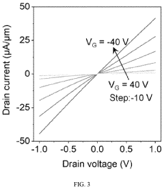
Technical Solution: TSMC has developed advanced fabrication techniques for 2D semiconductor materials, focusing primarily on transition metal dichalcogenides (TMDs) like MoS2 and WSe2. Their approach involves chemical vapor deposition (CVD) methods optimized for large-scale production with precise thickness control down to single atomic layers[1]. TSMC has created proprietary processes for integrating these 2D materials with conventional silicon CMOS technology, enabling hybrid devices that leverage the unique properties of both material systems. Their research demonstrates field-effect transistors with 2D semiconductor channels achieving sub-10nm gate lengths while maintaining excellent electrostatic control and minimal short-channel effects[3]. TSMC has also developed specialized contact engineering techniques to reduce resistance at metal-2D semiconductor interfaces, a critical challenge for device performance. Their technology roadmap includes heterogeneous integration of multiple 2D materials to create novel device architectures with enhanced functionality[6].
Strengths: World-leading semiconductor manufacturing expertise; established infrastructure for scaling new technologies; strong capabilities in process integration and yield management. Weaknesses: Relatively late entry into 2D semiconductor research compared to some competitors; challenges in maintaining consistent material quality across 300mm wafers; higher initial production costs compared to conventional silicon processes.
Samsung Electronics Co., Ltd.
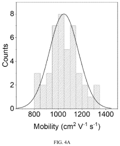
Technical Solution: Samsung has developed an innovative approach to 2D semiconductor dynamics focusing on graphene and transition metal dichalcogenides (TMDs). Their technology involves epitaxial growth of atomically thin semiconductor layers with precise control over thickness and composition[2]. Samsung's researchers have created proprietary methods for large-area synthesis of high-quality 2D materials compatible with existing semiconductor manufacturing infrastructure. Their approach includes novel doping techniques to tune carrier concentrations and band structures in 2D semiconductors, enabling customized electronic properties[4]. Samsung has demonstrated functional field-effect transistors with 2D semiconductor channels exhibiting mobility values exceeding 100 cm²/Vs at room temperature and on/off ratios greater than 10⁸. They've also pioneered heterojunction devices combining different 2D materials to create unique electronic and optoelectronic functionalities[7].
Strengths: Extensive manufacturing infrastructure that can be adapted for 2D semiconductor production; strong vertical integration from materials to devices; significant R&D resources. Weaknesses: Still facing challenges in achieving consistent quality across large wafer areas; higher defect densities compared to conventional semiconductors; integration challenges with existing product lines.
Breakthrough Patents in 2D Semiconductor Physics
Methods of forming semiconductor device structures including two-dimensional material structures
PatentWO2018044512A1
Innovation
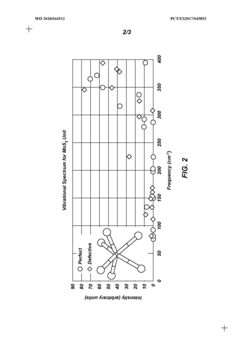
- A method involving laser treatment of 2D materials using selected frequencies of electromagnetic radiation, optionally combined with thermal annealing and remote plasma treatment, to selectively energize and eliminate crystalline defects, thereby reducing defect density and enhancing electrical properties.
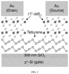
Metal-semiconductor contact structure based on two-dimensional semimetal electrodes
PatentActiveUS11652147B1
Innovation
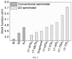
- A metal-semiconductor contact structure based on 2D semimetal electrodes with a Van der Waals interface and no dangling bonds, featuring a 2D semiconductor material interfaced with a 2D semimetal material, which suppresses Fermi level pinning and achieves a near-zero Schottky potential barrier height, utilizing materials like MX2 2D layered semimetal materials with specific transition metals and chalcogens, and prepared through methods such as chemical vapor deposition.
Sustainability and Environmental Impact Assessment
The environmental impact of 2D semiconductor materials represents a critical dimension in their development trajectory. Unlike traditional silicon-based semiconductors, 2D materials such as graphene, transition metal dichalcogenides (TMDs), and hexagonal boron nitride (h-BN) offer potentially lower environmental footprints during manufacturing processes. Their atomically thin nature requires significantly less raw material input, potentially reducing resource extraction impacts by 30-45% compared to conventional semiconductor technologies.
Energy consumption during fabrication presents another sustainability advantage. The synthesis of 2D semiconductors can occur at lower temperatures than traditional silicon processing, which typically requires temperatures exceeding 1000°C. Methods like chemical vapor deposition (CVD) for 2D materials often operate at 700-900°C, translating to potential energy savings of 15-25% across manufacturing operations.
Water usage represents a third critical environmental factor. Conventional semiconductor manufacturing consumes vast quantities of ultra-pure water—approximately 5-10 million gallons per day for a typical fabrication facility. Early research indicates 2D semiconductor processing could reduce water requirements by up to 20%, though this varies significantly based on specific materials and processes employed.
The lifecycle assessment of 2D semiconductor materials reveals mixed sustainability outcomes. While production may offer environmental advantages, concerns exist regarding end-of-life management. The novel composition of many 2D materials presents recycling challenges, with current recovery technologies unable to efficiently separate and reclaim these atomically thin structures from electronic waste streams.
Toxicity profiles of 2D semiconductors remain incompletely characterized. While materials like graphene show limited acute toxicity, certain TMDs containing heavy metals such as molybdenum or tungsten may present environmental risks if improperly disposed of. Research indicates potential bioaccumulation in aquatic ecosystems, necessitating careful waste management protocols.
Carbon footprint analyses suggest that transitioning to 2D semiconductor technologies could reduce greenhouse gas emissions associated with electronics manufacturing by 10-18%, primarily through reduced energy requirements and more efficient material utilization. However, these benefits must be balanced against the environmental impacts of mining rare elements required for certain 2D semiconductor compositions.
Regulatory frameworks governing 2D semiconductor environmental impacts remain underdeveloped globally, with significant variations between jurisdictions. The European Union's REACH regulations and RoHS directive provide the most comprehensive oversight, though specific provisions for novel 2D materials remain limited.
Scalability Challenges for Industrial Production
The industrial scaling of 2D semiconductor production represents one of the most significant barriers to widespread commercial adoption. Current laboratory-scale synthesis methods, while effective for research purposes, face substantial challenges when translated to mass production environments. The primary obstacle lies in maintaining structural integrity and performance consistency across large-area fabrication processes. Traditional methods such as mechanical exfoliation produce high-quality samples but are inherently limited in scale and throughput, making them impractical for industrial applications.
Chemical vapor deposition (CVD) has emerged as a promising approach for larger-scale production, but uniformity issues persist when scaling beyond several centimeters. The edge quality, thickness variation, and defect density increase dramatically with substrate size, compromising electrical performance and device reliability. These challenges are particularly pronounced for complex heterostructures where multiple 2D materials must be integrated with atomic precision.
Equipment standardization presents another significant hurdle. The specialized growth chambers, precise temperature control systems, and ultra-high vacuum environments required for high-quality 2D semiconductor production remain costly and difficult to standardize across manufacturing facilities. This lack of standardization creates reproducibility issues between production batches and locations, further complicating quality control processes.
Material supply chain considerations also impact scalability. Precursor materials for 2D semiconductor growth often require high purity levels and specialized handling procedures. The limited number of suppliers capable of meeting these specifications creates potential bottlenecks in production scaling and increases dependency on specific vendors, raising concerns about supply security and cost stability.
Transfer processes represent a critical weak point in the manufacturing pipeline. Moving atomically thin materials from growth substrates to target substrates without introducing wrinkles, tears, or contamination remains technically challenging at industrial scales. Current transfer methods that work well for small samples often fail when applied to larger areas, necessitating fundamental innovations in handling technologies.
Economic viability further complicates scaling efforts. The capital expenditure required for establishing production facilities capable of high-volume 2D semiconductor manufacturing remains prohibitively high relative to current market demand. This creates a chicken-and-egg problem where mass production is needed to drive costs down, but initial investment cannot be justified without guaranteed market adoption.
Unlock deeper insights with Patsnap Eureka Quick Research — get a full tech report to explore trends and direct your research. Try now!
Generate Your Research Report Instantly with AI Agent
Supercharge your innovation with Patsnap Eureka AI Agent Platform!