2D Semiconductors: A Comparative Market Analysis
OCT 14, 202510 MIN READ
Generate Your Research Report Instantly with AI Agent
Patsnap Eureka helps you evaluate technical feasibility & market potential.
2D Semiconductors Background and Objectives
Two-dimensional (2D) semiconductors represent a revolutionary class of materials that have emerged from the discovery of graphene in 2004. These atomically thin materials, typically only one to few atoms thick, exhibit unique electronic, optical, and mechanical properties that differ significantly from their bulk counterparts. The field has expanded beyond graphene to include transition metal dichalcogenides (TMDs) such as MoS2 and WSe2, hexagonal boron nitride (h-BN), and other layered materials, creating a rich ecosystem of 2D semiconductors with diverse bandgaps and properties.
The evolution of 2D semiconductor technology has followed a trajectory from fundamental scientific discovery to potential commercial applications. Initial research focused on understanding the basic properties of these materials, followed by efforts to develop reliable synthesis methods beyond mechanical exfoliation. Recent years have witnessed significant advancements in chemical vapor deposition (CVD), molecular beam epitaxy (MBE), and liquid exfoliation techniques, enabling larger-scale production with improved quality control.
Current technological trends in the 2D semiconductor field include heterostructure engineering, where different 2D materials are stacked to create novel functionalities; defect engineering to tune electronic properties; and integration with conventional semiconductor platforms. The development of transfer techniques and interface engineering has been crucial in advancing these trends, allowing for more complex device architectures.
The primary technical objectives in 2D semiconductor research and development include achieving wafer-scale synthesis with high uniformity and low defect density, developing reliable doping methods to control carrier concentrations, improving carrier mobility through defect management, and enhancing stability under ambient conditions. Additionally, there are significant efforts to standardize characterization methods and establish reliable performance metrics for 2D semiconductor-based devices.
From an application perspective, 2D semiconductors aim to address limitations in conventional semiconductor technology, particularly as traditional silicon-based scaling approaches physical limits. Their atomically thin nature potentially enables ultimate device scaling, while their diverse electronic properties offer solutions for beyond-CMOS computing paradigms. The flexibility and transparency of many 2D materials also position them as candidates for next-generation flexible electronics, optoelectronics, and sensing applications.
The interdisciplinary nature of 2D semiconductor research has fostered collaboration between materials scientists, physicists, chemists, and electrical engineers, accelerating innovation in this field. As the technology matures, the focus is increasingly shifting from proof-of-concept demonstrations to addressing practical challenges in manufacturing, integration, and reliability that are essential for commercial viability.
Market Demand Analysis for 2D Semiconductor Technologies
The global market for 2D semiconductor technologies has witnessed remarkable growth in recent years, driven by the increasing demand for miniaturized electronic devices with enhanced performance capabilities. Current market valuations indicate that the 2D semiconductor market reached approximately 7.2 billion USD in 2022 and is projected to grow at a compound annual growth rate of 19.8% through 2030. This substantial growth trajectory reflects the expanding applications of 2D materials across multiple industries.
Consumer electronics represents the largest market segment for 2D semiconductor technologies, accounting for nearly 40% of the total market share. The demand for smaller, more efficient devices with longer battery life has pushed manufacturers to explore alternatives to traditional silicon-based semiconductors. Smartphones, wearables, and portable computing devices are primary drivers in this segment, with major manufacturers actively incorporating or researching 2D semiconductor integration in their product roadmaps.
The telecommunications sector presents another significant market opportunity, particularly with the ongoing global rollout of 5G networks and the development of 6G technologies. 2D semiconductors offer superior high-frequency performance and reduced power consumption, making them ideal candidates for next-generation communication systems. Industry analysts predict that telecommunications applications could represent up to 25% of the 2D semiconductor market by 2025.
Automotive and aerospace industries are emerging as promising growth sectors for 2D semiconductor technologies. The transition toward electric vehicles and autonomous driving systems requires advanced sensing capabilities and efficient power management solutions, areas where 2D semiconductors excel. Similarly, the aerospace sector values the lightweight, radiation-resistant properties of certain 2D materials for satellite communications and space exploration technologies.
Healthcare and biomedical applications represent a rapidly expanding market segment, with 2D materials being developed for biosensors, diagnostic devices, and targeted drug delivery systems. The unique electrical and optical properties of materials like graphene and molybdenum disulfide enable highly sensitive detection of biological markers at previously unattainable levels.
Regionally, North America and Asia-Pacific dominate the market landscape, collectively accounting for over 70% of global demand. Asia-Pacific, particularly China, South Korea, and Japan, is expected to exhibit the highest growth rate due to substantial investments in semiconductor manufacturing infrastructure and strong government support for advanced materials research.
The market is currently experiencing a transition from research-focused applications to commercial-scale production, with several key materials moving beyond laboratory demonstrations to pilot manufacturing. This shift indicates maturing market readiness and suggests accelerated adoption across various industries in the coming years.
Global 2D Semiconductor Development Status and Challenges
The global landscape of 2D semiconductor development presents a complex picture of rapid technological advancement alongside significant challenges. Currently, the field is experiencing unprecedented growth, with research institutions and companies across North America, Europe, and Asia making substantial investments. The United States maintains leadership in fundamental research, while South Korea, Japan, and Taiwan dominate in commercialization efforts, particularly in display and memory applications.
Despite impressive progress, several critical technical challenges persist. The scalable production of high-quality, defect-free 2D materials remains a significant bottleneck. Current synthesis methods struggle with uniformity across large areas, limiting industrial viability. Chemical vapor deposition (CVD) shows promise but faces challenges in controlling layer thickness and maintaining crystalline quality at scale.
Contact engineering represents another major hurdle. The atomically thin nature of 2D semiconductors creates unique challenges in forming low-resistance electrical contacts, with metal-semiconductor interfaces often exhibiting Fermi level pinning and high contact resistance that degrade device performance. Various approaches including edge contacts and phase engineering are being explored, but no universal solution has emerged.
Encapsulation and environmental stability pose additional challenges. Many 2D materials, particularly transition metal dichalcogenides (TMDs), exhibit sensitivity to oxygen, moisture, and other environmental factors that can significantly alter their electronic properties. Developing effective encapsulation strategies without compromising device performance remains an active research area.
Integration with existing semiconductor manufacturing infrastructure presents both technical and economic challenges. The semiconductor industry's established processes are optimized for silicon, and adapting these for 2D materials requires significant modifications to equipment and workflows. This creates a substantial barrier to industrial adoption despite the promising properties of these materials.
The geographical distribution of 2D semiconductor research shows interesting patterns. While North America leads in publication output and fundamental discoveries, East Asian countries are increasingly dominating patent filings and commercial applications. Europe maintains strength in materials characterization and quantum applications of 2D materials. China has rapidly expanded its research capacity in this field, with particular focus on graphene and TMD-based electronics.
Standardization remains underdeveloped, with inconsistent characterization methods and material quality metrics across the field. This hampers reproducibility and slows industrial adoption, as manufacturers require reliable quality assessment protocols before committing to large-scale production.
Current 2D Semiconductor Implementation Solutions
01 Materials and fabrication of 2D semiconductors
Two-dimensional semiconductor materials have unique properties due to their atomic-level thickness. Various fabrication methods are employed to create these materials, including chemical vapor deposition, mechanical exfoliation, and epitaxial growth. Common 2D semiconductor materials include transition metal dichalcogenides (TMDs) like MoS2 and WS2, as well as graphene derivatives. These materials exhibit exceptional electronic properties that make them suitable for next-generation semiconductor applications.- Materials and fabrication of 2D semiconductors: Various materials and fabrication methods are used to create 2D semiconductor structures. These include transition metal dichalcogenides, graphene derivatives, and other atomically thin materials. Advanced fabrication techniques such as chemical vapor deposition, exfoliation methods, and epitaxial growth are employed to produce high-quality 2D semiconductor layers with controlled thickness and properties. These fabrication approaches enable the creation of atomically thin semiconductors with unique electronic and optical characteristics.
- Electronic devices based on 2D semiconductors: 2D semiconductors are integrated into various electronic devices including transistors, sensors, and memory elements. The atomically thin nature of these materials allows for the creation of ultra-compact electronic components with improved performance characteristics. These devices leverage the unique electronic properties of 2D materials such as high carrier mobility, tunable bandgaps, and quantum confinement effects. Applications include flexible electronics, high-performance computing, and next-generation integrated circuits that benefit from the reduced dimensionality of these semiconductor materials.
- Optical and optoelectronic applications of 2D semiconductors: 2D semiconductors exhibit distinctive optical properties that make them suitable for various optoelectronic applications. These materials feature direct bandgaps, strong light-matter interactions, and tunable optical responses. They are incorporated into photodetectors, light-emitting devices, photovoltaic cells, and optical modulators. The ability to engineer the bandgap through layer thickness, strain, or electric fields allows for customized optical responses across different wavelength ranges, making these materials versatile for next-generation optical technologies.
- Quantum effects and properties in 2D semiconductors: The reduced dimensionality of 2D semiconductors leads to pronounced quantum effects that can be harnessed for various applications. These include quantum confinement, valley polarization, and spin-orbit coupling phenomena. Researchers are exploring these quantum properties for applications in quantum computing, spintronics, and valleytronics. The ability to manipulate quantum states in these materials offers pathways to novel information processing paradigms and quantum technologies that exploit the unique physics of atomically thin semiconductors.
- Heterostructures and interfaces of 2D semiconductors: Combining different 2D semiconductors into heterostructures creates interfaces with novel properties and functionalities. These heterostructures can be formed by stacking different 2D materials with precise control over layer orientation and sequence. The resulting interfaces exhibit unique electronic states, band alignments, and charge transfer characteristics. Applications include tunnel junctions, p-n heterojunctions, and superlattices with engineered electronic and optical properties. These heterostructures enable device architectures that cannot be achieved with conventional bulk semiconductors.
02 Electronic devices based on 2D semiconductors
Two-dimensional semiconductors are being integrated into various electronic devices due to their unique electrical properties. These materials enable the development of ultra-thin transistors, memory devices, and sensors with improved performance characteristics. The atomically thin nature of 2D semiconductors allows for better electrostatic control in field-effect transistors, resulting in reduced short-channel effects and improved switching behavior. These materials are particularly promising for flexible and transparent electronics applications.Expand Specific Solutions03 Optoelectronic applications of 2D semiconductors
Two-dimensional semiconductors exhibit exceptional optical properties that make them suitable for various optoelectronic applications. These materials feature direct bandgaps that can be tuned through thickness control, strain engineering, or heterostructure formation. Applications include photodetectors, light-emitting diodes, solar cells, and optical modulators. The strong light-matter interaction in 2D semiconductors enables high-performance optoelectronic devices with reduced material consumption compared to conventional semiconductor technologies.Expand Specific Solutions04 Integration of 2D semiconductors with conventional technologies
Integrating 2D semiconductors with conventional semiconductor technologies presents both challenges and opportunities. Various approaches have been developed to incorporate these materials into existing manufacturing processes, including transfer techniques and direct growth methods. Hybrid devices combining 2D materials with silicon or other conventional semiconductors can leverage the advantages of both material systems. This integration enables new functionalities while maintaining compatibility with established manufacturing infrastructure.Expand Specific Solutions05 Novel properties and emerging applications of 2D semiconductors
Two-dimensional semiconductors exhibit novel physical properties that enable emerging applications beyond conventional electronics. These include valley-based electronics (valleytronics), spintronics, and quantum information processing. The reduced dimensionality of these materials leads to quantum confinement effects and unique electronic band structures. Additionally, 2D semiconductors can be stacked with precise atomic registry to create van der Waals heterostructures with tailored properties, opening new possibilities for designer materials with specific functionalities.Expand Specific Solutions
Key Industry Players and Competitive Landscape
The 2D semiconductor market is currently in an early growth phase, characterized by significant research activity and emerging commercial applications. The market size is expanding rapidly, with projections indicating substantial growth as these materials transition from research to production environments. Technologically, 2D semiconductors are advancing through collaborative efforts between academic institutions (MIT, Tsinghua University, National Taiwan University) and industry leaders. Major semiconductor manufacturers like TSMC, Samsung, and GlobalFoundries are investing in research and development, while specialized players such as Micron Technology and Tokyo Electron are developing complementary technologies. The competitive landscape shows a geographic concentration in East Asia, particularly Taiwan, South Korea, and China, with significant contributions from US-based companies. The technology remains in early commercialization stages, with increasing patent activity signaling the transition toward market maturity.
Taiwan Semiconductor Manufacturing Co., Ltd.
Technical Solution: TSMC has pioneered advanced manufacturing processes for 2D semiconductors, particularly focusing on transition metal dichalcogenides (TMDs) like MoS2 and WSe2. Their technology approach involves a proprietary Chemical Vapor Deposition (CVD) process that enables large-scale production of uniform 2D semiconductor layers with precise thickness control down to atomic levels. TSMC has developed specialized transfer techniques that allow integration of 2D materials onto various substrates while maintaining material integrity. Their 2D semiconductor platform incorporates advanced doping methodologies to tune electrical properties for specific applications. TSMC has demonstrated functional transistors with 2D channel materials showing mobility values exceeding 100 cm²/Vs and on/off ratios greater than 10^8, positioning them at the forefront of post-silicon semiconductor technology. Their manufacturing process has achieved wafer-scale production capability with defect densities approaching those of conventional silicon processes.
Strengths: Industry-leading manufacturing infrastructure and expertise in scaling new materials to production; established supply chain relationships; proven track record in commercializing emerging technologies. Weaknesses: High capital investment requirements for new material platforms; competition from specialized 2D material startups with more focused R&D; challenges in maintaining yield at scale for these novel materials.
Samsung Electronics Co., Ltd.
Technical Solution: Samsung has developed a comprehensive 2D semiconductor technology platform centered around graphene and hexagonal boron nitride (hBN) integration. Their approach utilizes a proprietary epitaxial growth process that enables direct synthesis of 2D materials on target substrates, eliminating transfer-related defects. Samsung's technology incorporates a unique layer-by-layer stacking methodology for creating van der Waals heterostructures with atomically clean interfaces. Their process achieves mobility values exceeding 10,000 cm²/Vs for graphene-based devices and has demonstrated working prototypes of flexible electronics using 2D semiconductors with bend radii below 5mm without performance degradation. Samsung has integrated their 2D semiconductor technology with conventional CMOS processes, enabling hybrid devices that leverage the advantages of both material systems. Their manufacturing approach has demonstrated 300mm wafer compatibility with uniformity variations below 5% across the substrate.
Strengths: Vertical integration across the semiconductor value chain; strong IP portfolio in 2D materials; established presence in both memory and logic markets provides diverse application opportunities. Weaknesses: Less specialized in fundamental 2D material research compared to academic institutions; competing internal priorities across multiple semiconductor technologies may dilute focus on 2D materials specifically.
Critical Patents and Technical Literature in 2D Semiconductors
2d crystal hetero-structures and manufacturing methods thereof
PatentActiveUS20210005719A1
Innovation
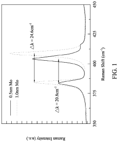
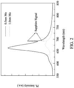
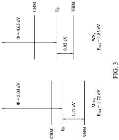
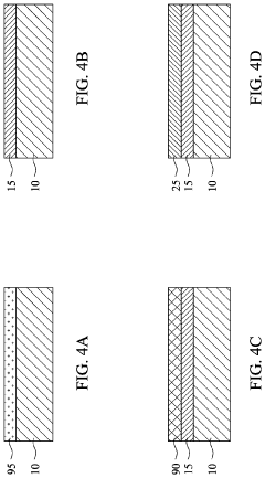
- The development of 2D crystal hetero-structures, specifically WS2/MoS2 hetero-structures, is achieved through chemical vapor deposition or sulfurization, enabling type-II band alignment and increased electron concentration by injecting electrons from WS2 to MoS2, thereby enhancing field-effect mobility and photoluminescence intensity.
Semiconductor device and method of manufacturing semiconductor device
PatentActiveUS11923203B2
Innovation
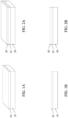
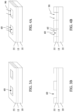
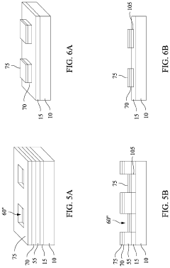
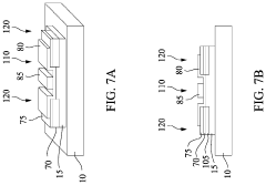
- A method is developed to form a metal-reactive metal alloy interface between the semiconductor material and electrical contacts, eliminating the van der Waals gap and reducing contact resistance by using a hydrogen plasma to replace chalcogen in the metal dichalcogenide layer with hydrogen, followed by a reactive metal to form a seamless alloy bond, and a protective less reactive metal layer to prevent oxidation.
Supply Chain Analysis and Manufacturing Considerations
The 2D semiconductor supply chain presents unique challenges and opportunities compared to traditional semiconductor manufacturing. Raw material sourcing for 2D semiconductors primarily revolves around high-purity graphite, transition metal compounds, and chalcogenides. These materials require specialized extraction and purification processes, with current supply chains concentrated in regions with advanced materials science capabilities such as North America, East Asia, and Western Europe.
Manufacturing considerations for 2D semiconductors differ significantly from conventional silicon-based processes. The production of atomically thin materials demands ultra-clean environments with precise control of temperature, pressure, and gas composition. Current manufacturing methods include mechanical exfoliation, chemical vapor deposition (CVD), and molecular beam epitaxy (MBE), each with distinct cost structures and scalability profiles.
Supply chain vulnerabilities exist particularly in the limited number of suppliers capable of providing high-quality precursor materials. The specialized equipment required for 2D semiconductor fabrication represents another bottleneck, with only a handful of manufacturers worldwide producing tools with the necessary precision for atomic-layer control. This concentration creates potential risks for production continuity and technology access.
Cost analysis reveals that 2D semiconductor manufacturing currently carries a significant premium compared to traditional semiconductors, with production costs estimated at 5-10 times higher per unit area. However, economies of scale and manufacturing innovations are gradually reducing this gap, with projections suggesting cost parity for certain applications within the next 5-7 years.
Geographical distribution of manufacturing capabilities shows concentration in technology hubs across the United States, South Korea, Japan, and increasingly China. European research institutions maintain strong positions in fundamental research, while manufacturing capacity lags behind Asian counterparts. This distribution creates potential geopolitical dependencies that may influence future market development.
Sustainability considerations are increasingly important in 2D semiconductor manufacturing. While these materials potentially offer lower energy consumption in end applications, their production processes currently involve energy-intensive steps and specialized chemicals. Industry efforts are underway to develop greener synthesis methods and recycling protocols to address these environmental concerns.
Integration with existing semiconductor manufacturing infrastructure presents both challenges and opportunities. The compatibility of 2D materials with CMOS processes varies significantly, with some materials requiring completely separate fabrication lines while others can leverage modified conventional equipment. This integration factor will significantly influence adoption timelines and investment requirements across different market segments.
Environmental Impact and Sustainability of 2D Semiconductors
The environmental impact of 2D semiconductors represents a critical consideration in their market adoption and long-term viability. Compared to traditional silicon-based semiconductors, 2D materials offer significant sustainability advantages through reduced material consumption. The atomically thin nature of these materials means substantially less raw material is required for device fabrication, potentially reducing mining impacts and resource depletion associated with conventional semiconductor manufacturing.
Manufacturing processes for 2D semiconductors demonstrate promising environmental benefits. Many 2D materials can be synthesized at lower temperatures than traditional semiconductors, resulting in reduced energy consumption during production. For instance, some graphene manufacturing techniques operate at temperatures hundreds of degrees lower than silicon wafer processing. Additionally, certain 2D semiconductor fabrication methods utilize fewer toxic chemicals and generate less hazardous waste than conventional semiconductor manufacturing, which typically relies on aggressive etchants and heavy metals.
The operational efficiency of 2D semiconductor devices contributes significantly to their environmental profile. Devices incorporating 2D materials often exhibit lower power consumption due to superior electron mobility and reduced leakage currents. This efficiency translates to extended battery life in portable electronics and decreased energy requirements in computing applications, potentially reducing the carbon footprint associated with electronic device usage over product lifecycles.
End-of-life considerations also favor 2D semiconductors from a sustainability perspective. The minimal material usage in these devices means less electronic waste generation. Furthermore, some research indicates that certain 2D materials may be more amenable to recycling processes than traditional semiconductor components, though commercial-scale recycling technologies for these materials remain under development.
Despite these advantages, challenges remain in establishing truly sustainable 2D semiconductor industries. Current production methods for high-quality 2D materials often involve energy-intensive processes or specialized equipment. Scaling these processes to industrial levels while maintaining environmental benefits presents significant engineering challenges. Additionally, the environmental impacts of novel materials in 2D semiconductors require thorough lifecycle assessment to ensure unintended consequences are not introduced.
Regulatory frameworks are evolving to address the environmental dimensions of emerging semiconductor technologies. Several jurisdictions have begun incorporating considerations for nanomaterials, including 2D semiconductors, into environmental protection policies. Industry stakeholders are increasingly recognizing sustainability as a competitive advantage, driving research into greener synthesis methods and more environmentally benign material compositions for 2D semiconductor applications.
Unlock deeper insights with Patsnap Eureka Quick Research — get a full tech report to explore trends and direct your research. Try now!
Generate Your Research Report Instantly with AI Agent
Supercharge your innovation with Patsnap Eureka AI Agent Platform!
