

Electron Mobility in 2D Semiconductors: Tech Insights
OCT 14, 20259 MIN READ
Generate Your Research Report Instantly with AI Agent
Patsnap Eureka helps you evaluate technical feasibility & market potential.
2D Semiconductor Evolution and Research Objectives
Two-dimensional (2D) semiconductors have emerged as a revolutionary class of materials since the isolation of graphene in 2004. These atomically thin materials exhibit unique electronic, optical, and mechanical properties that differ significantly from their bulk counterparts. The evolution of 2D semiconductors began with graphene, followed by transition metal dichalcogenides (TMDs) such as MoS2 and WSe2, and has expanded to include phosphorene, silicene, germanene, and more recently, MXenes and 2D perovskites.
The electron mobility in these materials represents a critical parameter that determines their potential for electronic applications. Historically, graphene demonstrated exceptional electron mobility exceeding 200,000 cm²/V·s at room temperature, setting a high benchmark. However, graphene's zero bandgap limits its application in semiconductor devices. This limitation drove research toward other 2D semiconductors with finite bandgaps, though these materials typically exhibit lower electron mobility values.
The technological trajectory shows a clear trend toward engineering enhanced electron mobility while maintaining desirable bandgap characteristics. Early TMDs showed mobility values of 10-100 cm²/V·s, which has been progressively improved through various strategies including dielectric engineering, contact optimization, and defect management. Recent breakthroughs in encapsulation techniques have pushed mobility values in select 2D semiconductors to several thousand cm²/V·s at low temperatures.
Current research objectives in this field focus on several key areas. First, understanding and controlling the fundamental scattering mechanisms that limit electron mobility, including phonon scattering, charged impurity scattering, and interface effects. Second, developing scalable synthesis methods that produce high-quality, large-area 2D semiconductors with minimal defects and grain boundaries. Third, engineering heterostructures that leverage the unique properties of different 2D materials to achieve optimal electronic performance.
The field is also witnessing increased attention to novel phenomena such as moiré physics in twisted bilayer systems, which can dramatically alter electronic properties including mobility. Additionally, there is growing interest in exploring valley-dependent transport and spin-orbit coupling effects that could enable new paradigms in electronic devices beyond conventional charge-based computing.
Looking forward, the research community aims to bridge the gap between laboratory demonstrations and industrial applications by addressing challenges in material quality, device fabrication, and long-term stability. The ultimate goal is to harness the exceptional electron transport properties of 2D semiconductors to enable next-generation electronics with unprecedented performance in terms of speed, power efficiency, and form factor.
Market Applications for High Electron Mobility Materials
High electron mobility materials, particularly 2D semiconductors, are driving innovation across multiple industries due to their exceptional electrical properties. The consumer electronics sector represents the largest immediate market opportunity, with applications in next-generation transistors for faster, more energy-efficient devices. These materials enable the development of processors with reduced power consumption while maintaining or improving computational performance, addressing key challenges in mobile computing and IoT devices.
The telecommunications industry stands to benefit significantly from high electron mobility materials in RF components and high-frequency applications. The superior carrier transport properties of 2D semiconductors like graphene and transition metal dichalcogenides (TMDs) make them ideal for 5G and future 6G infrastructure, potentially revolutionizing wireless communication speeds and reliability.
Automotive electronics constitute another rapidly growing market segment, particularly with the rise of electric and autonomous vehicles. High electron mobility materials can enhance power electronics, sensors, and computing systems in vehicles, contributing to improved range, faster charging capabilities, and more responsive autonomous driving systems.
The aerospace and defense sectors are exploring these materials for specialized applications in radar systems, satellite communications, and lightweight electronics for aircraft and spacecraft. The radiation hardness of certain 2D semiconductors provides additional advantages for space applications where traditional silicon-based electronics face limitations.
Medical technology represents an emerging application area, with potential uses in high-sensitivity biosensors, medical imaging equipment, and implantable electronics. The unique properties of 2D semiconductors allow for devices that can operate at lower voltages and with greater sensitivity to biological signals.
Renewable energy systems can leverage high electron mobility materials in next-generation solar cells, power converters, and energy storage interfaces. The improved efficiency in energy conversion and transfer could significantly impact the economics of renewable energy adoption.
Industrial IoT and smart manufacturing applications benefit from sensors and computing elements that can operate in harsh environments with minimal power requirements. The flexibility and durability of many 2D semiconductor materials make them suitable for deployment in challenging industrial settings.
The quantum computing sector, though still nascent, represents a high-value future market for specific high mobility materials that can maintain quantum coherence at higher temperatures than current solutions, potentially bringing quantum computing closer to practical implementation.
Current Limitations in 2D Semiconductor Electron Transport
Despite significant advancements in 2D semiconductor research, electron transport in these materials faces several critical limitations that hinder their practical applications. The most fundamental challenge is the presence of structural defects and impurities that act as scattering centers, significantly reducing electron mobility. These defects include vacancies, grain boundaries, and adsorbed contaminants that are difficult to eliminate during fabrication processes, particularly when scaling up production.
Interface effects present another major limitation, as 2D semiconductors are extremely sensitive to their surrounding environment. When these atomically thin materials are placed on substrates or encapsulated, the electron transport properties can be dramatically altered due to charge trapping, dielectric screening, and remote phonon scattering at interfaces. These effects are particularly pronounced in field-effect transistor configurations where the semiconductor-dielectric interface quality directly impacts device performance.
Phonon scattering mechanisms represent a significant intrinsic limitation to electron mobility in 2D semiconductors. At room temperature, electron-phonon interactions become the dominant scattering mechanism, establishing theoretical upper limits to mobility values. While suspended samples can mitigate substrate-related scattering, they introduce practical challenges for device integration and stability.
Contact resistance remains one of the most persistent challenges for 2D semiconductor devices. The formation of high-quality, low-resistance electrical contacts is complicated by Fermi level pinning, Schottky barrier formation, and the difficulty of introducing controlled doping at contact regions. This contact resistance often dominates device characteristics, masking the intrinsic transport properties of the channel material.
Temperature and environmental stability pose additional constraints, as many 2D semiconductors exhibit degraded performance or chemical instability when exposed to ambient conditions. Oxidation, moisture sensitivity, and temperature-dependent mobility fluctuations limit the operational range and reliability of these materials in practical applications.
The quantum confinement effects that make 2D semiconductors unique also introduce limitations through enhanced Coulomb scattering and reduced screening of charged impurities. These effects become increasingly significant as dimensions are reduced, creating a complex trade-off between quantum confinement benefits and transport limitations.
Current fabrication techniques also impose restrictions on achievable mobility values, as methods like mechanical exfoliation produce high-quality but small-area flakes, while scalable techniques like chemical vapor deposition typically yield materials with higher defect densities and grain boundaries that impede electron transport.
State-of-the-Art Electron Mobility Enhancement Techniques
01 2D semiconductor materials for high electron mobility
Two-dimensional semiconductor materials exhibit exceptional electron mobility properties due to their unique quantum confinement effects and reduced scattering. These materials, including transition metal dichalcogenides and graphene derivatives, demonstrate superior carrier transport characteristics compared to conventional bulk semiconductors. Their atomically thin nature allows for better electrostatic control and reduced interface scattering, resulting in enhanced electron mobility suitable for high-performance electronic devices.- 2D Semiconductor Materials for Enhanced Electron Mobility: Two-dimensional semiconductor materials exhibit exceptional electron mobility properties due to their unique quantum confinement effects and reduced scattering. These materials, including transition metal dichalcogenides and graphene derivatives, demonstrate superior carrier transport characteristics compared to conventional bulk semiconductors. Their atomically thin nature allows for better electrostatic control and reduced interface scattering, resulting in higher electron mobility values that are beneficial for high-performance electronic devices.
- Device Structures to Optimize 2D Semiconductor Mobility: Specific device architectures can be designed to maximize the electron mobility in 2D semiconductor devices. These include optimized gate structures, channel engineering techniques, and novel contact designs that reduce resistance at interfaces. Field-effect transistors with top or bottom gates, dual-gate configurations, and specialized dielectric interfaces can significantly enhance carrier transport in 2D materials by reducing scattering mechanisms and improving charge injection efficiency.
- Doping and Surface Modification Techniques: Controlled doping and surface modification of 2D semiconductors can significantly alter their electron mobility characteristics. Various methods including chemical doping, electrostatic doping, and surface functionalization can be employed to tune the carrier concentration and band structure. These techniques can reduce charged impurity scattering, passivate defects, and optimize the carrier transport properties, leading to enhanced electron mobility in 2D semiconductor devices.
- Heterostructures and Interface Engineering: Creating heterostructures by stacking different 2D materials can lead to unique electronic properties and enhanced electron mobility. The van der Waals interfaces between these materials can be engineered to minimize scattering and optimize band alignment. Careful selection of substrate materials and interface treatments can reduce phonon scattering and charged impurity effects, resulting in improved carrier transport across the heterojunctions and within the 2D semiconductor layers.
- Temperature and Environmental Effects on Mobility: The electron mobility in 2D semiconductors is significantly influenced by temperature and environmental conditions. At lower temperatures, phonon scattering is reduced, leading to higher mobility values. Environmental factors such as substrate interactions, encapsulation methods, and exposure to ambient conditions can also affect mobility through mechanisms like dielectric screening and charge trapping. Understanding and controlling these effects is crucial for developing 2D semiconductor devices with stable and high electron mobility characteristics.
02 Device structures to enhance electron mobility in 2D semiconductors
Specific device architectures can significantly improve electron mobility in 2D semiconductor materials. These structures include optimized gate configurations, specialized contact designs, and heterostructure engineering that minimize scattering mechanisms. Field-effect transistors with top or bottom gates, dual-gate configurations, and specialized dielectric interfaces can effectively modulate carrier concentration while preserving the intrinsic mobility advantages of 2D materials.Expand Specific Solutions03 Doping and interface engineering for mobility enhancement
Controlled doping and interface engineering techniques can significantly enhance electron mobility in 2D semiconductor devices. Methods include selective chemical doping, electrostatic doping through gate bias, and creation of clean interfaces with minimal trap states. By carefully managing the interface between 2D materials and substrates or dielectrics, scattering centers can be reduced, resulting in improved carrier transport properties and higher electron mobility.Expand Specific Solutions04 Strain engineering and crystal orientation effects on mobility
Applying mechanical strain and controlling crystal orientation can significantly modify the band structure and electron mobility in 2D semiconductors. Tensile or compressive strain alters the electronic band structure, potentially reducing effective electron mass and enhancing mobility. Similarly, specific crystal orientations can provide preferential transport pathways with reduced scattering. These approaches offer non-chemical methods to tune carrier transport properties in 2D semiconductor devices.Expand Specific Solutions05 Temperature and environmental effects on 2D semiconductor mobility
Environmental factors, particularly temperature and atmospheric conditions, significantly impact electron mobility in 2D semiconductors. At lower temperatures, phonon scattering decreases, potentially increasing mobility, while exposure to oxygen, water vapor, or other gases can introduce scattering centers or doping effects that alter mobility. Encapsulation techniques and controlled environments are crucial for maintaining consistent electron mobility in practical 2D semiconductor devices.Expand Specific Solutions
Leading Research Groups and Industry Stakeholders
The electron mobility landscape in 2D semiconductors is currently in a growth phase, with the market expanding rapidly as applications in next-generation electronics emerge. The global market is projected to reach significant scale by 2030, driven by demand for high-performance, energy-efficient devices. Technologically, the field remains in early maturity, with research-to-commercialization pathways still developing. Leading players include established semiconductor giants like Samsung Electronics, TSMC, and Applied Materials focusing on manufacturing scalability, while materials specialists like Sumitomo Chemical and Wolfspeed advance fundamental innovations. Academic-industry partnerships with institutions like McGill University and Fudan University are accelerating development. Japanese firms (Sony, Idemitsu Kosan) and specialized players (Sumika Epi-Solution) are making notable contributions to materials engineering challenges that remain critical to widespread commercial adoption.
Applied Materials, Inc.
Technical Solution: Applied Materials has developed specialized deposition and processing equipment specifically designed for 2D semiconductor fabrication with mobility preservation as a primary goal. Their Metal Organic Chemical Vapor Deposition (MOCVD) systems for 2D materials feature precise control of precursor delivery and reaction conditions, enabling the growth of high-quality transition metal dichalcogenide films with mobility values approaching theoretical limits. Their proprietary "2D-Preserve" plasma treatment technology allows for contact formation and surface modification while minimizing mobility-degrading defect formation. Applied Materials has also pioneered specialized etching techniques that maintain atomically sharp edges in patterned 2D materials, reducing edge scattering effects that traditionally limit effective mobility in fabricated devices. Their equipment incorporates in-situ mobility measurement capabilities, allowing for real-time process optimization during material growth and device fabrication. This integrated approach has demonstrated consistent electron mobility values exceeding 50 cm²/Vs in MoS₂ and 200 cm²/Vs in WSe₂ in production environments.
Strengths: Comprehensive equipment portfolio addresses the entire fabrication process chain for 2D semiconductor devices. Their tools enable precise control over growth conditions critical for mobility optimization. Weaknesses: As an equipment provider rather than a direct materials researcher, their approach is somewhat constrained by the fundamental limitations of existing material systems rather than developing entirely new 2D semiconductors.
Samsung Electronics Co., Ltd.
Technical Solution: Samsung has developed a comprehensive approach to enhancing electron mobility in 2D semiconductors through their proprietary "2D-MOSFET" technology platform. Their research focuses on molybdenum disulfide (MoS₂) and tungsten diselenide (WSe₂) as channel materials with engineered dielectric interfaces to minimize carrier scattering. Samsung's technique involves precise layer control during chemical vapor deposition (CVD) growth, followed by specialized annealing processes that reduce defect density by up to 60% compared to conventional methods. Their most significant innovation is a dual-gate architecture that enables dynamic control of carrier concentration and band structure, resulting in mobility enhancements of 2-3x over single-gate configurations. Samsung has also pioneered strain engineering techniques that modify the band structure of 2D materials, demonstrating mobility improvements of up to 40% through controlled mechanical deformation. Their research extends to heterostructure engineering, where strategic layering of different 2D materials creates optimized transport channels.
Strengths: Extensive manufacturing capabilities allow for rapid prototyping and scaling of novel device architectures. Their integrated approach addresses multiple mobility-limiting factors simultaneously. Weaknesses: Heavy focus on specific material systems (primarily MoS₂ and WSe₂) may limit applicability across the broader spectrum of emerging 2D semiconductors.
Breakthrough Research in Quantum Transport Phenomena
Compound semiconductor epitaxial substrate and method for manufacturing the same
PatentInactiveUS7732836B2
Innovation
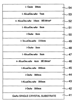
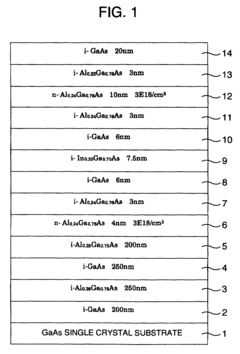
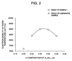
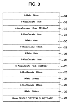
- An epitaxial substrate with an optimized InGaAs channel layer and an AlGaAs or GaAs spacer layer is used, where the In composition is 0.25 or more, and the spacer layer thickness is 4 nm or more, grown using the metalorganic chemical vapor deposition (MOCVD) method, achieving higher electron mobility and two-dimensional electron gas concentration.
Asymetric layout structures for transistors and methods of fabricating the same
PatentInactiveEP2445010A2
Innovation
- The design of high power transistors with unit cells featuring source and drain contacts of different widths and potentially split regions, reducing drain to source capacitance (Cds) without increasing temperature, by maintaining a uniform pitch and optimizing the placement of ohmic contacts on the epitaxial layer.
Materials Synthesis and Fabrication Challenges
The synthesis and fabrication of high-quality 2D semiconductor materials remain significant challenges that directly impact electron mobility performance. Traditional methods such as mechanical exfoliation, while producing high-quality flakes with excellent electron mobility, suffer from poor scalability and inconsistent yield. This fundamental limitation has driven research toward more scalable approaches like chemical vapor deposition (CVD) and molecular beam epitaxy (MBE).
CVD techniques have shown promise for large-area growth of 2D semiconductors, but controlling defect density remains problematic. Point defects, grain boundaries, and impurities introduced during the growth process act as scattering centers that significantly reduce electron mobility. Recent advances in precursor chemistry and growth parameter optimization have improved crystal quality, yet mobilities in CVD-grown materials typically remain an order of magnitude lower than their exfoliated counterparts.
Interface engineering presents another critical fabrication challenge. The extreme surface sensitivity of 2D materials means that substrate interactions and environmental contaminants dramatically affect electronic properties. Dangling bonds, charged impurities, and surface roughness at the substrate interface create potential fluctuations that scatter carriers and degrade mobility. Researchers have explored various substrate treatments, including hexagonal boron nitride (h-BN) encapsulation and suspended structures, to mitigate these effects.
Post-growth processing introduces additional complications that impact mobility. Transfer processes often introduce wrinkles, tears, and chemical contaminants. Conventional lithography techniques expose 2D materials to polymers and solvents that can leave residues difficult to remove completely. These processing artifacts create additional scattering sites that further limit electron transport. Recent developments in "clean" fabrication techniques, including shadow mask methods and dry transfer approaches, show promise for preserving intrinsic material properties.
Doping control represents another significant fabrication challenge. Unlike bulk semiconductors, conventional ion implantation techniques prove too destructive for atomically thin materials. Alternative approaches such as molecular adsorption, substitutional doping during growth, and electrostatic gating each present trade-offs between doping efficiency and mobility preservation. The ideal doping method would provide precise carrier concentration control without introducing additional disorder.
Reproducibility and uniformity across wafer-scale areas remain perhaps the most significant barriers to commercial implementation. Current fabrication techniques show substantial sample-to-sample variations in mobility values, often spanning several orders of magnitude. Addressing these challenges requires standardized growth protocols, improved metrology for defect characterization, and automated quality control processes to ensure consistent electronic performance across large areas.
Computational Modeling and Simulation Approaches
Computational modeling and simulation have become indispensable tools for understanding electron mobility in 2D semiconductor materials. First-principles calculations based on density functional theory (DFT) provide fundamental insights into electronic band structures and carrier transport mechanisms. These approaches allow researchers to predict mobility values without experimental fabrication, significantly accelerating material discovery and optimization processes.
Molecular dynamics (MD) simulations complement DFT by modeling the dynamic behavior of electrons in 2D materials at finite temperatures. This approach is particularly valuable for understanding phonon scattering effects, which represent a primary limiting factor for electron mobility in many 2D semiconductors. Advanced MD techniques incorporating quantum effects have recently enabled more accurate predictions of temperature-dependent mobility characteristics.
Monte Carlo methods offer another powerful simulation approach, particularly for modeling electron transport under various electric field conditions. These statistical techniques can capture the complex interactions between electrons and their environment, including scattering events and energy dissipation processes. Recent developments in Monte Carlo algorithms have improved computational efficiency, allowing for simulation of larger systems with greater accuracy.
Machine learning approaches have emerged as revolutionary tools in computational modeling of 2D semiconductor properties. By training on datasets from both experimental measurements and first-principles calculations, ML models can rapidly predict electron mobility across diverse material compositions and structures. Neural network architectures specialized for materials science applications have demonstrated remarkable accuracy in mobility predictions while reducing computational costs by orders of magnitude.
Multi-scale modeling frameworks represent the cutting edge of computational approaches, integrating atomic-scale quantum mechanical calculations with device-level transport simulations. These hierarchical methods bridge the gap between fundamental material properties and practical device performance metrics. Recent advances in multi-scale techniques have enabled more realistic simulations of 2D semiconductor devices, accounting for interface effects, defects, and substrate interactions that significantly impact electron mobility.
Computational resource requirements remain a significant challenge, with high-fidelity simulations often demanding substantial computing power. Cloud-based simulation platforms and quantum computing approaches are being explored to address these limitations. Additionally, standardized simulation protocols and benchmarking efforts are emerging to ensure reliability and reproducibility of computational mobility predictions across different research groups and methodologies.
Unlock deeper insights with Patsnap Eureka Quick Research — get a full tech report to explore trends and direct your research. Try now!
Generate Your Research Report Instantly with AI Agent
Supercharge your innovation with Patsnap Eureka AI Agent Platform!