

2D Semiconductor Adoption in Emerging Electronics
OCT 14, 202510 MIN READ
Generate Your Research Report Instantly with AI Agent
Patsnap Eureka helps you evaluate technical feasibility & market potential.
2D Semiconductor Evolution and Objectives
Two-dimensional (2D) semiconductors represent a revolutionary class of materials that have emerged from the discovery of graphene in 2004. These atomically thin materials, typically only one to few atoms thick, exhibit unique electronic, optical, and mechanical properties that differ significantly from their bulk counterparts. The evolution of 2D semiconductors began with graphene's isolation, which demonstrated exceptional electron mobility and mechanical strength but lacked a natural bandgap—a critical requirement for semiconductor applications. This limitation prompted researchers to explore beyond graphene, leading to the discovery of transition metal dichalcogenides (TMDs) such as MoS2, WS2, and other layered materials that possess natural bandgaps suitable for electronic applications.
The technological trajectory of 2D semiconductors has been marked by significant milestones over the past decade. Following initial material discoveries, research focus shifted toward developing reliable synthesis methods, from mechanical exfoliation to chemical vapor deposition (CVD) and molecular beam epitaxy (MBE), enabling larger-scale production with improved quality control. Concurrently, characterization techniques advanced to probe these materials' unique properties at the atomic scale, facilitating deeper understanding of their behavior and potential applications.
Recent years have witnessed accelerated progress in heterostructure engineering—the strategic stacking of different 2D materials to create novel functionalities through quantum confinement and interlayer interactions. This approach has opened pathways to designer materials with tailored electronic and optical properties, expanding the application landscape beyond conventional semiconductor capabilities.
The primary objective of 2D semiconductor research and development is to harness their exceptional properties to overcome the fundamental limitations of traditional silicon-based electronics. As conventional semiconductor scaling approaches physical limits, 2D materials offer a promising alternative with their atomically precise thickness, excellent carrier transport properties, and mechanical flexibility. Specific technical goals include developing reliable large-scale synthesis methods, improving material quality and uniformity, enhancing carrier mobility while maintaining stability, and establishing industry-compatible integration processes.
Looking forward, the field aims to enable practical applications across multiple domains: ultra-scaled logic devices that extend Moore's Law beyond silicon's limitations; flexible and transparent electronics for wearable technology; highly sensitive sensors for environmental and biomedical applications; and energy-efficient optoelectronic devices. The ultimate objective is to transition 2D semiconductors from laboratory curiosities to commercially viable technologies that address emerging needs in computing, communications, healthcare, and energy sectors, potentially revolutionizing the electronics industry through fundamentally new device architectures and functionalities.
Market Demand Analysis for 2D Semiconductor Applications
The global market for 2D semiconductors is experiencing rapid growth, driven by increasing demand for miniaturized electronic devices with enhanced performance capabilities. Current market analysis indicates that the 2D semiconductor market is projected to grow at a compound annual growth rate of 30% through 2030, significantly outpacing the broader semiconductor industry's growth rate of 4-6%.
Consumer electronics represents the largest application segment for 2D semiconductors, accounting for approximately 40% of the total market demand. This is primarily fueled by the integration of 2D materials like graphene, molybdenum disulfide, and hexagonal boron nitride in next-generation smartphones, wearables, and portable computing devices. The ultra-thin profile and exceptional electrical properties of these materials enable manufacturers to develop increasingly compact devices with improved battery life and processing capabilities.
The automotive sector has emerged as the fastest-growing market segment for 2D semiconductors, with demand increasing by 45% annually. This surge is attributed to the accelerating adoption of electric vehicles and advanced driver-assistance systems, which require high-performance, energy-efficient semiconductors capable of operating reliably under demanding conditions. 2D semiconductors offer significant advantages in thermal management and power efficiency, making them particularly valuable for automotive applications.
Healthcare and biomedical applications represent another promising market for 2D semiconductors, particularly in biosensing and diagnostic equipment. The exceptional sensitivity of 2D materials to environmental changes makes them ideal for developing highly accurate biosensors capable of detecting minute concentrations of biomarkers. Market research indicates that the biomedical segment for 2D semiconductors is growing at 35% annually, driven by increasing investment in personalized medicine and point-of-care diagnostics.
Regional analysis reveals that Asia-Pacific currently dominates the 2D semiconductor market with a 45% share, followed by North America (30%) and Europe (20%). However, the most rapid growth is occurring in emerging economies, particularly in Southeast Asia and India, where expanding manufacturing capabilities and government initiatives to develop domestic semiconductor industries are creating new market opportunities.
Industry surveys indicate that key customer requirements driving 2D semiconductor adoption include improved energy efficiency (cited by 78% of respondents), reduced form factor (65%), enhanced processing speed (60%), and lower production costs (55%). These market demands align well with the inherent advantages of 2D semiconductors, suggesting strong potential for continued market expansion as manufacturing processes mature and production scales increase.
Current Challenges in 2D Semiconductor Implementation
Despite the promising properties of 2D semiconductors, their widespread implementation faces significant technical challenges. The atomically thin nature of these materials, while advantageous for certain applications, creates substantial difficulties in manufacturing processes. Current fabrication techniques struggle to produce large-area, defect-free 2D semiconductor sheets at industrial scales. The presence of grain boundaries, wrinkles, and atomic vacancies significantly impacts electrical performance and device reliability.
Contact resistance remains a critical bottleneck in 2D semiconductor devices. The atomically thin profile of these materials creates unique challenges at metal-semiconductor interfaces, resulting in high contact resistance that limits current flow and overall device performance. Traditional contact engineering approaches developed for silicon technology are often ineffective for 2D materials due to their distinct surface properties and lack of dangling bonds.
Encapsulation and environmental stability present ongoing challenges. Many 2D semiconductors, particularly transition metal dichalcogenides (TMDs), exhibit sensitivity to ambient conditions including oxygen and moisture. This environmental sensitivity leads to performance degradation over time and complicates both manufacturing and operational reliability. Current encapsulation solutions often compromise the inherent advantages of 2D materials by increasing device thickness or introducing additional interfaces.
Integration with existing semiconductor manufacturing infrastructure poses significant hurdles. The established semiconductor industry relies heavily on silicon-optimized processes that may damage or contaminate 2D materials. Adapting these processes or developing entirely new ones compatible with 2D semiconductors requires substantial investment and technical innovation. The temperature sensitivity of many 2D materials further complicates their integration into standard back-end-of-line processes.
Doping control and carrier mobility optimization remain technically challenging. Unlike conventional semiconductors, traditional doping methods are difficult to implement in 2D materials due to their ultrathin nature. Current approaches often result in unintentional doping or material degradation. Additionally, while theoretical mobility values for pristine 2D semiconductors are impressive, practical devices frequently exhibit significantly lower performance due to scattering mechanisms at interfaces, substrate interactions, and material defects.
Heterogeneous integration of different 2D materials to create functional device stacks introduces additional complexity. The weak van der Waals forces between layers create challenges in achieving precise alignment and maintaining interface quality. Current transfer techniques often introduce contaminants or damage that degrade device performance. These integration challenges become particularly acute when attempting to scale production beyond laboratory demonstrations to commercial manufacturing volumes.
Current 2D Semiconductor Integration Solutions
01 2D semiconductor materials and fabrication
Two-dimensional semiconductor materials have unique electronic properties due to their atomic-scale thickness. These materials, including transition metal dichalcogenides, graphene derivatives, and other layered structures, can be fabricated through various methods such as chemical vapor deposition, exfoliation, and epitaxial growth. The fabrication processes are designed to control thickness, crystallinity, and defect density, which directly impact the electronic performance of these materials.- 2D semiconductor materials and fabrication: Two-dimensional semiconductor materials have unique electronic properties due to their atomic-scale thickness. These materials, including transition metal dichalcogenides, graphene derivatives, and other layered structures, can be fabricated through various methods such as chemical vapor deposition, exfoliation, or epitaxial growth. The fabrication processes focus on achieving high-quality, uniform layers with controlled thickness and minimal defects to optimize their semiconductor properties.
- Electronic devices using 2D semiconductors: Two-dimensional semiconductors are increasingly being incorporated into various electronic devices due to their exceptional electrical properties and ultrathin profiles. These materials enable the development of next-generation transistors, memory devices, sensors, and integrated circuits with improved performance characteristics. The unique band structures and carrier transport properties of 2D semiconductors allow for devices with higher efficiency, flexibility, and novel functionalities compared to traditional semiconductor technologies.
- Optical and optoelectronic applications of 2D semiconductors: Two-dimensional semiconductors exhibit distinctive optical properties that make them valuable for optoelectronic applications. Their direct bandgaps and strong light-matter interactions enable efficient light emission, absorption, and modulation. These materials are being developed for applications in photodetectors, light-emitting diodes, photovoltaics, and optical modulators. The tunable bandgap of many 2D semiconductors allows for customization across different wavelengths of the electromagnetic spectrum.
- Heterostructures and interfaces of 2D semiconductors: Combining different 2D semiconductor materials into heterostructures creates unique electronic and optical properties at their interfaces. These heterostructures can be designed with atomic precision by stacking different 2D materials, allowing for band engineering and novel quantum phenomena. The interfaces between 2D semiconductors and other materials (including 3D semiconductors) are crucial for device integration and performance optimization, enabling new functionalities not achievable with single-material systems.
- Processing and integration technologies for 2D semiconductors: Specialized processing and integration technologies are required to incorporate 2D semiconductors into practical devices and systems. These include techniques for large-area synthesis, transfer methods, contact engineering, and integration with conventional semiconductor manufacturing processes. Challenges such as minimizing contamination, controlling interface quality, and ensuring reproducibility are addressed through innovative processing approaches that enable the commercial viability of 2D semiconductor technologies.
02 Electronic devices based on 2D semiconductors
Two-dimensional semiconductors enable the development of ultra-thin electronic devices with superior performance characteristics. These materials are incorporated into transistors, memory devices, sensors, and integrated circuits. The atomic thinness of 2D semiconductors allows for better electrostatic control, reduced short-channel effects, and potentially higher carrier mobility compared to conventional bulk semiconductors, making them promising candidates for next-generation electronics.Expand Specific Solutions03 Optoelectronic applications of 2D semiconductors
Two-dimensional semiconductors exhibit distinctive optical properties that make them suitable for various optoelectronic applications. Their direct bandgap nature (in many cases) enables efficient light emission and absorption. These materials are used in photodetectors, light-emitting diodes, photovoltaic cells, and optical modulators. The bandgap tunability through layer number control, strain engineering, or heterostructure formation provides versatility in designing optoelectronic devices with specific wavelength responses.Expand Specific Solutions04 Heterostructures and interfaces in 2D semiconductors
Vertical stacking of different 2D materials creates heterostructures with novel properties not found in individual layers. These heterostructures enable band alignment engineering, interlayer excitons, and quantum confinement effects. The atomically sharp interfaces between different 2D materials minimize defects and dangling bonds, allowing for clean electronic interfaces. Various combinations of semiconducting, metallic, and insulating 2D materials can be used to create functional devices with tailored electronic properties.Expand Specific Solutions05 Integration of 2D semiconductors with conventional technologies
Integrating 2D semiconductors with conventional semiconductor technologies presents both challenges and opportunities. Methods for incorporating these materials into existing fabrication processes include transfer techniques, direct growth, and hybrid integration approaches. Compatibility issues with traditional processing steps, such as high-temperature treatments and chemical exposures, must be addressed. The integration enables hybrid devices that combine the advantages of 2D materials with mature silicon technology, potentially leading to enhanced performance in computing, sensing, and communication applications.Expand Specific Solutions
Key Industry Players and Competitive Landscape
The 2D semiconductor market is in a growth phase, with increasing adoption in emerging electronics driven by demand for smaller, more efficient devices. The market is projected to expand significantly as applications in flexible electronics, IoT, and advanced computing develop. Technologically, industry leaders like Taiwan Semiconductor Manufacturing Co., Samsung Electronics, and Intel are advancing commercial viability, while Huawei and SiOnyx are developing innovative applications. Academic institutions including MIT, Korea Advanced Institute of Science & Technology, and National Taiwan University are conducting fundamental research to overcome challenges in mass production, stability, and integration. The ecosystem shows a collaborative dynamic between established semiconductor manufacturers, emerging technology companies, and research institutions working to transition 2D semiconductors from laboratory to mainstream applications.
Taiwan Semiconductor Manufacturing Co., Ltd.
Technical Solution: TSMC has pioneered the integration of 2D semiconductors into its advanced manufacturing processes, focusing primarily on transition metal dichalcogenides (TMDs) like MoS2 and WSe2. Their approach involves developing specialized deposition techniques for creating uniform, large-area 2D materials compatible with existing CMOS processes. TSMC has established a dedicated 2D materials research division that collaborates with academic institutions to overcome manufacturing challenges. Their technology roadmap includes incorporating 2D semiconductors as channel materials in sub-3nm nodes, leveraging the atomically thin nature of these materials to extend Moore's Law beyond silicon's physical limitations[1]. TSMC has demonstrated functional transistors with 2D semiconductor channels showing improved electrostatic control and reduced short-channel effects compared to conventional silicon devices[3].
Strengths: Industry-leading manufacturing infrastructure, established supply chain integration capabilities, and extensive R&D resources. Weaknesses: High implementation costs for new material integration and challenges in achieving consistent quality across large wafer areas for 2D semiconductor deposition.
Samsung Electronics Co., Ltd.
Technical Solution: Samsung has developed a comprehensive approach to 2D semiconductor adoption focusing on both memory and logic applications. Their technology centers on graphene and hexagonal boron nitride (hBN) heterostructures for next-generation electronics. Samsung's Advanced Institute of Technology has pioneered methods for large-scale synthesis of 2D materials using chemical vapor deposition (CVD) optimized for 300mm wafer compatibility[2]. Their proprietary transfer techniques minimize contamination and defects when integrating 2D materials with conventional semiconductor platforms. Samsung has demonstrated functional prototypes of memory devices utilizing 2D materials as selector elements, achieving switching ratios exceeding 10^6 with significantly lower power consumption than conventional technologies[4]. Their roadmap includes commercialization of hybrid 2D/3D integrated circuits by 2025.
Strengths: Vertical integration across the semiconductor value chain, strong IP portfolio in 2D materials, and established mass production capabilities. Weaknesses: Challenges in achieving consistent electrical properties across large-area 2D films and higher initial manufacturing costs compared to conventional semiconductor technologies.
Critical Patents and Research in 2D Semiconductor Field
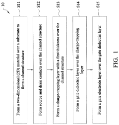
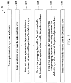
Impact ionization semiconductor device and manufacturing method thereof
PatentActiveUS20200119204A1
Innovation
- The introduction of a charge-trapping layer near the source region facilitates the trapping of minority carriers, creating a positive feedback mechanism that reduces contact resistance and enhances current flow by improving the subthreshold slope and lowering contact resistance through impact ionization and charge trapping.
Supply Chain Considerations for 2D Semiconductor Production
The establishment of a robust and efficient supply chain is critical for the successful commercialization of 2D semiconductor technologies. Current supply chain structures for 2D semiconductor production remain fragmented and underdeveloped compared to traditional silicon-based semiconductor manufacturing ecosystems. This presents both challenges and opportunities for industry stakeholders.
Material sourcing represents a primary concern in the 2D semiconductor supply chain. High-quality precursors and substrates are essential for producing 2D materials with consistent properties. Currently, the supply of these materials is limited to specialized chemical suppliers and research institutions, resulting in high costs and variable quality. Establishing reliable sources for key materials such as transition metal dichalcogenides (TMDs), graphene, and hexagonal boron nitride (h-BN) will be crucial for scaling production.
Manufacturing processes for 2D semiconductors differ significantly from conventional semiconductor fabrication. While traditional semiconductor manufacturing relies on well-established processes like chemical vapor deposition (CVD) and physical vapor deposition (PVD), 2D semiconductor production often requires specialized techniques such as mechanical exfoliation, chemical vapor transport (CVT), and molecular beam epitaxy (MBE). The equipment supply chain for these processes is currently limited, with few vendors offering specialized tools optimized for 2D material production.
Integration challenges further complicate the supply chain landscape. 2D semiconductors must eventually interface with conventional electronics, requiring specialized packaging and integration solutions. The current ecosystem lacks standardized approaches for integrating 2D materials with silicon platforms, creating bottlenecks in the production pipeline.
Geographical considerations also impact supply chain development. Currently, research and production capabilities for 2D semiconductors are concentrated in North America, Europe, and East Asia. This concentration creates potential vulnerabilities in the supply chain, particularly regarding critical materials that may be sourced from regions with geopolitical instability.
Scaling production represents perhaps the most significant supply chain challenge. Moving from laboratory-scale production to industrial volumes requires substantial investment in manufacturing infrastructure. The capital-intensive nature of semiconductor fabrication facilities (fabs) presents barriers to entry for new players, potentially limiting innovation and competition in the space.
Collaborative ecosystem development will be essential for addressing these supply chain challenges. Industry consortia, academic-industrial partnerships, and government initiatives can help establish standards, share resources, and distribute development costs across multiple stakeholders. Such collaborative approaches will be critical for building the robust supply chain infrastructure necessary to support widespread adoption of 2D semiconductor technologies in emerging electronics applications.
Environmental Impact and Sustainability Factors
The adoption of 2D semiconductors in emerging electronics presents significant environmental and sustainability advantages compared to traditional semiconductor materials. These atomically thin materials require substantially less raw material input during manufacturing, directly reducing resource extraction impacts. The minimal material usage translates to lower energy consumption during production processes, with some studies indicating potential energy savings of 30-45% compared to conventional silicon-based manufacturing.
2D semiconductor fabrication processes generally involve fewer toxic chemicals and hazardous substances than traditional semiconductor manufacturing. Materials like graphene, molybdenum disulfide (MoS2), and hexagonal boron nitride (h-BN) can be synthesized through cleaner methods such as chemical vapor deposition and mechanical exfoliation, reducing the environmental footprint associated with harsh chemical processes.
The extended lifecycle of 2D semiconductor-based devices represents another sustainability advantage. Their superior electrical properties enable more efficient power management, resulting in devices that consume less energy during operation. Research indicates that electronics incorporating 2D semiconductors can achieve power reductions of up to 70% in certain applications, significantly extending battery life and reducing overall energy consumption throughout the product lifecycle.
End-of-life considerations also favor 2D semiconductor technologies. Their minimal material usage simplifies recycling processes, while their composition often excludes many rare earth elements that pose recycling challenges in conventional electronics. This characteristic aligns with circular economy principles and addresses growing concerns about electronic waste management.
Carbon footprint analyses of 2D semiconductor manufacturing show promising results, with potential reductions of 25-40% in greenhouse gas emissions compared to traditional semiconductor production. This advantage becomes increasingly significant as the electronics industry faces mounting pressure to reduce its environmental impact amid global climate change mitigation efforts.
Water usage represents another critical sustainability factor. Conventional semiconductor manufacturing is notoriously water-intensive, consuming thousands of gallons per wafer produced. Early studies suggest 2D semiconductor production could reduce water requirements by 35-50%, addressing a growing concern in regions facing water scarcity challenges.
Despite these advantages, challenges remain in scaling 2D semiconductor production sustainably. Current laboratory-scale synthesis methods must evolve to maintain their environmental benefits at industrial scales. Additionally, comprehensive lifecycle assessments are needed to fully quantify the environmental advantages and identify potential unforeseen impacts as adoption increases across the electronics industry.
Unlock deeper insights with Patsnap Eureka Quick Research — get a full tech report to explore trends and direct your research. Try now!
Generate Your Research Report Instantly with AI Agent
Supercharge your innovation with Patsnap Eureka AI Agent Platform!